Driving an SPI device using MPSSE
Synchronous protocols: MPSSE
In a synchronous protocol (such as SPI or I2C) both clock and data signals are transmitted from sender to receiver, so the two remain in sync. This is in contrast to asynchronous (e.g. RS-232) protocols where markers in the data are used to establish & maintain sync.
The newer FTDI chips have a very strong capability in this area, which they call Multi-Protocol Synchronous Serial Engine, or MPSSE. This mode is enabled by the same command we use to enable bitbanging; the first argument is unused, and the second argument has the value 2 for MPSSE.
d.ftdi_fn.ftdi_set_bitmode(0, 2) # MPSSE using pylibftdi or..
d.setBitMode(0, 2)               # ..using ftd2xx
Bits 0 and 1 are chosen as outputs since they are normally SPI clock and data out; see part 1 for information on I/O pins usage.
Once MPSSE is set up, it is controlled by reading & writing byte streams; command bytes with optional arguments and data. The commands are detailed in FTDI application note 108 ‘Command Processor for MPSSE and MCU Host Bus Emulation Modes’, and at first sight there appears to be a bewildering array of options; the key to understanding them is that each command is actually a bitfield, namely:
Bit   MPSSE Function      If set    If clear
0     Write clock edge    -ve       +ve
1     Bit/byte mode       bit       byte
2     Read clock edge     -ve       +ve
3     LS/MS bit first     LS        MS
4     TDI/DO data output  On        Off
5     TDO/DI data input   On        Off
6     TMS data output     On        Off
7     Zero
On a normal microcontroller serial interface you set up the transfer parameters (clock edge, bit-order, word-length) in advance, then just do byte or word transfers based on those settings. The FTDI interface is completely different; the parameters are specified for each transfer, and you can freely intersperse commands with different word-lengths, clock edges etc. Bits 4 -6 are particularly strange, in that they allow you to control the flow of data to & from the chip; if just bit 4 is set you have a write-only interface, just bit 5 and it is read-only. What use is that? Very useful, if we’re doing more complex protocols such as SWD, but for simpler read/write tasks you’d probably want to leave DO & DI enabled (not TMS, unless you’re implementing JTAG) .
These serial-data commands have bit 7 clear, but the FTDI application note describes various other commands that are available if bit 7 is set; for example, to set an I/O pin in MPSSE mode the following commands are used:
Command   Data bytes    Action
80h       Value, Mask   Write low byte (ADBUS)
82h       Value, Mask   Write high byte (ACBUS)
81h                     Read low byte (ADBUS)
83h                     Read high byte (ACBUS)
For serial output we need to set the SPI clock and MOSI pins (bits 0 & 1) to be outputs, so the command to be sent is:
OPS = 0x03
ft_write(d, (0x80, 0, OPS))
This makes the clock & MOSI lines into outputs, with a value of 0
MPSSE example: SPI output
The MPSSE command structure is easiest to explain with a worked example, and since SPI (Serial Peripheral Interface) is the simplest clocked serial protocol it supports, we’ll start with that.
SPI normally has 4 lines; clock, data out, data in, and chip-select. Since it can be ambiguous as to which direction ‘out’ and ‘in’ refer to, those terms are normally qualified as MOSI (Master Out Slave In) and MISO (Master In Slave Out). The chip-select is used to mark the beginning and end of a transaction, and to identify which chip is being addressed out of (potentially) several chips on the bus.
For this example I’ll be using SPI to drive a MAX6969 LED driver chip; this is used in various low-cost multiple-LED displays, in this case the MikroElektronika UT-L 7-SEG R click with dual 7-segment displays.

This can be set to select 3.3 or 5 volt operation by re-soldering a resistor; to save this complication, we’ll leave it in the default 3.3V mode. That means we need an FTDI module with 3.3V outputs, since they must match the supply voltage – if you doubt this, check the ‘absolute maximum’ values in the MAX6969 data sheet.

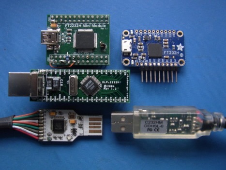
With a supply of 3.3V, the data and clock inputs can only go 0.3V higher before bad things happen – you ignore Absolute Maximum ratings at your peril. So our FTDI interface needs to be 3.3V; any such module with MPSSE capability will do, I’ll use the C232HM-DDHSL-0 cable.
It can only supply a maximum current of 200 mA to the power-hungry display module; lighting 16 segments at around 20 mA each will easily overload this supply, so we need an external 3.3V source, with at least 0.5A capacity. The connections are:
Display pin  Function      FTDI cable  Function
3            Load Enable   Grey        GPIOL0 (ADBUS4)
4            Clock         Orange      TCK
5            Data out      Green       TDO
6            Data in       Yellow      TDI
7            3.3V
8 & 9        Ground        Black       GND
16           PWM           Brown       TMS (ADBUS3)
It may look like I’ve got the input and output lines the wrong way round, but FTDI are using the device-oriented JTAG pin identifiers, so TDO is actually MISO, and TDI is MOSI.
Pin 3 ‘load enable’ is similar to ‘chip enable’, and is connected to an I/O line that can be toggled; we’ll be looking at its exact function later. Pin 16 is a line that can be used to vary the display brightness using pulse-width modulation; it must be driven high to illuminate the display.
When first using new hardware, it is well worth checking the supply current with an ammeter, and making a note of it; this board takes 4 mA at 3.3V; not a lot!
Device configuration
The default data rate is less than ideal for our application, so we need to set something better; 1 MHz is a good safe starting-point for most SPI devices. Command 86 hex sets the data rate, followed by the low byte and high byte of the frequency divisor (which turns out to be 5 for 1 MHz).
hz = 1000000                            # Desired SPI frequency
div = int((12000000 / (hz * 2)) - 1)
ft_write(d, (0x86, div%256, div//256))  # Return byte count (3)
Now we can write some data to the SPI interface, and view the result on an oscilloscope. According to the MPSSE function table , a command value of 10h will send a byte value to DO, with +ve clocks, M.S.Bit first. After the command byte, you send a word value, L.S.Byte first, that tells the command how long the data is, minus 1 byte; in this case, we’re sending 1 byte of SPI data with value 55h, so the whole command in hex is 10 00 00 55
def ft_write_cmd_bytes(d, cmd, data):
    n = len(data) - 1
    ft_write(d, [cmd, n%256, n//256] + list(data))
#
# Set bit 0 & 1 (TCK, TDI) as O/Ps, output 1 byte: 55h
SPI_MASK = 3
ft_write(d, (0x80, SPI_MASK, SPI_MASK))
ft_write_cmd_bytes(d, 0x10, [0x55])
This is the resulting oscilloscope display

In case you aren’t used to looking round an oscilloscope display, the top figures say what the vertical & horizontal sensitivities are, in units per division (i.e. units per large square). So the data and clock lines are 2 volts per division vertically, which looks roughly right, since we’re expecting 3.3V signals. The horizontal scale is 2 microseconds per division, which also looks right, since we get 2 clock cycles per division, so each cycle has a period of 1 microsecond, corresponding to a frequency of 1MHz.
You’ll also see that the data line changes at the same time as the clock line goes from low to high, i.e. at the positive-going clock edge. This is to be expected since bit 0 if the command (‘write clock edge’) is set to zero (‘+ve’). This is important because the display chip will be using a specific clock edge to read in the data bits, and if we have chosen the wrong edge, the data will be changing while it is being read in, with highly unpredictable results. The relevant text in the MAX6969 data sheet says “DIN is the serial-data input, and must be stable when it is sampled on the rising edge of CLK”.
So we need to set command bit 0 so that the data changes on the falling clock edge, and is stable on the rising edge. There are also 2 other issues to address:
- The ‘load enable’ pin must be toggled to latch the data into the display after it has been sent. This is somewhat unusual, since normally a chip-enable signal is asserted before the data is sent, and negated afterwards, but we do need to toggle the load-enable line or nothing will be visible.
- The PWM signal needs to be asserted to illuminate the display. It is intended to be driven from a pulse-width-modulated (PWM) signal to give variable intensity, but since we don’t have that, needs to be turned full-on.
So here is our next attempt, writing 2 bytes (one for each display) with data changing on negative edge, latching the transferred data, and turning on the display.
OE, LE = 0x08, 0x10
ft_write(d, (0x80, 0, OPS+OE+LE))         # Set outputs
ft_write_cmd_bytes(d, 0x11, (0x3f, 0x06)) # Write seg data
ft_write(d, (0x80, LE, OPS+OE+LE))        # Latch = 1
ft_write(d, (0x80, OE, OPS+OE+LE))        # Latch = 0, disp = 1
ft_write(d, (0x80, 0,  OPS+OE+LE))        # Latch = disp = 0
If all is well, the number 10 appears on the display when it is enabled. How did I know that the hex values 3F and 06 were needed to display 0 and 1? Rather than work out the segment-to-I/O-bit mapping for myself, I just looked at the C code on the MikroElektronik Web page, that gave the values for 0 – 9, and copied the first 2.
Here is the resulting waveform; it is quite instructive to match the bit values with the high/low states of the MOSI line.

Avoiding disaster
An earlier version of the SPI write code looked like this:
ft_write(d, (0x80, OPS, OPS))
ft_write_cmd_bytes(d, 0x11, (0x3f, 0x06))
Looks quite harmless, but the oscilloscope showed a major problem; see the highlighted areas on the clock trace.

There are some sizeable glitches in our clock signal, which is very bad news. Will the MAX6969 chip see these pulses, or ignore them, and if they are accepted, will a high or low level be read in? Having glitches like this on the clock line is very risky; even if it works now, it could suddenly stop working with a minor rearrangement of the components or wiring.
The solution is to set the outputs to zero when enabling MPSSE mode:
ft_write(d, (0x80, 0, OPS))
ft_write_cmd_bytes(d, 0x11, (0x3f, 0x06))
This issue demonstrates how a software bug has the potential to create a subtle hardware problem; it is always worth checking the waveforms with an oscilloscope, if at all possible.
Source code
Here is the source code, tested on Windows using the D2XX driver, and Linux using pylibftdi – just set the FTD2XX value appropriately.
# Python FTDI SPI example from iosoft.blog
# Compatible with Python 2.7 or 3.x
# Drives a MikroElektronika UT-L 7-SEG R display
#
# v0.01 JPB 8/12/18

FTD2XX       = True  # Set False if using pylibftdi
FTDI_TIMEOUT = 1000  # Timeout for D2XX read/write (msec)

if FTD2XX:
    import sys, time, ftd2xx as ftd
else:
    import sys, time, pylibftdi as ftdi

# Segment bit values for digits 0 - 9
dig_segs = 0x3F,0x06,0x5B,0x4F,0x66,0x6D,0x7D,0x07,0x7F,0x6F

DIG1 = 0    # Digits to be displayed
DIG2 = 1
OPS  = 0x03 # Bit mask for SPI clock and data out
OE   = 0x08 #              display output enable
LE   = 0x10 #              display latch enable

# Set mode (bitbang / MPSSE)
def set_bitmode(d, bits, mode):
    return (d.setBitMode(bits, mode) if FTD2XX else
            d.ftdi_fn.ftdi_set_bitmode(bits, mode))

# Open device for read/write
def ft_open(n=0):
    if FTD2XX:
        d = ftd.open(n)
        d.setTimeouts(FTDI_TIMEOUT, FTDI_TIMEOUT)
    else:
        d = ftdi.Device(device_index=n)
    return d

# Set SPI clock rate
def set_spi_clock(d, hz):
    div = int((12000000 / (hz * 2)) - 1)  # Set SPI clock
    ft_write(d, (0x86, div%256, div//256))

# Read byte data into list of integers
def ft_read(d, nbytes):
    s = d.read(nbytes)
    return [ord(c) for c in s] if type(s) is str else list(s)

# Write list of integers as byte data
def ft_write(d, data):
    s = str(bytearray(data)) if sys.version_info<(3,) else bytes(data)
    return d.write(s)

# Write MPSSE command with word-value argument
def ft_write_cmd_bytes(d, cmd, data):
    n = len(data) - 1
    ft_write(d, [cmd, n%256, n//256] + list(data))

if __name__ == "__main__":
    dev = ft_open(0)
    if dev:
        print("FTDI device opened")
        set_bitmode(dev, OPS, 2)              # Set SPI mode
        set_spi_clock(dev, 1000000)           # Set SPI clock
        ft_write(dev, (0x80, 0, OPS+OE+LE))   # Set outputs
        data = dig_segs[DIG1], dig_segs[DIG2] # Convert digits to segs
        ft_write_cmd_bytes(dev, 0x11, data)   # Write seg bit data
        ft_write(dev, (0x80, LE, OPS+OE+LE))  # Latch = 1
        ft_write(dev, (0x80, OE, OPS+OE+LE))  # Latch = 0, disp = 1
        print("Displaying '%u%u'" % (DIG2, DIG1))
        time.sleep(1)
        ft_write(dev, (0x80, 0,  OPS+OE+LE))  # Latch = disp = 0
        print("Display off")
        dev.close()
# EOF
See the next post for an introduction to the SWD protocol.
Copyright (c) Jeremy P Bentham 2018. Please credit this blog if you use the information or software in it.
 Lean2
Lean2 