In a previous post, I described ‘EDLA’, a WiFi-based logic analyser unit, that uses a Web-based display. That version used an ESP32 to provide WiFi connectivity; the PEDLA uses a Pi PicoW module instead.
Hardware
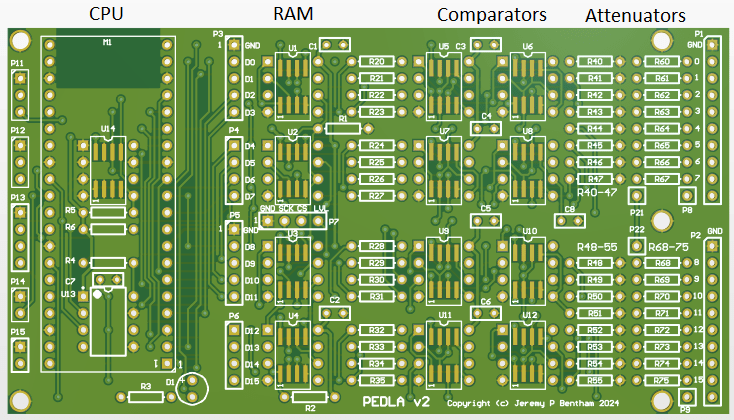
PEDLA circuit board
The hardware is similar to the previous version; aside from the CPU change, the main addition is a 24LC256 serial EEPROM, that is used to store the non-volatile configuration parameters. The Pico flash memory can’t be used for this task, since it is bulk-erased at the start of every programming cycle. The parameters are set using a simple serial console interface.
Firmware
The firmware is written in C; networking is implemented using the picowi WiFi driver, combined with the Mongoose TCP/IP stack; follow these links for more information. The source code is on github here.
Copyright (c) Jeremy P Bentham 2024. Please credit this blog if you use the information or software in it.
Analog signal capture at 60 megasamples per second
This project provides a simple way of capturing data using a Pi PicoW, and displaying it wirelessly on a Web browser, as either as a logic analyser, or an oscilloscope.
The digital capture is done using the Pico I/O lines; the analogue capture uses an AD9226 parallel ADC module, that can provide up to 65 megasamples per second. The same firmware is used for both; for speed, the data is sent over the network as raw 16-bit values.
Hardware
In its simplest form, the only hardware required is a Pi PicoW module.
Minimal logic analyser circuit diagram
This can monitor 16 (or more) input lines, but it is essential that the voltage remains between 0 and 3.3V, otherwise damage will result. To accommodate wider voltages, an attenuator & comparator can be used, as in the EDLA project.
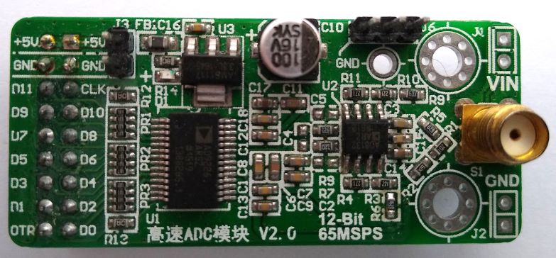
High-speed analog input uses a AD9226 ADC module, that is readily available online.
AD9226 module
It requires a 5V supply, but can be directly connected to the Pico I/O lines.
Minimal analog capture circuit diagram
Although the ADC has 12-bit resolution, only 10 bits have been used. It is possible to use all 12 bits, with minor changes to the software.
Note that some AD9226 modules have the most-significant pin marked as D0, not D11; if in doubt refer to the device datasheet, and do a continuity check between the IC pins and the I/O connections.
The ADC clock pin is connected to two I/O lines; the clock is generated on GPIO22, and read back on GPIO17. The latter is used to track the number of pulses emitted, using the pulse-counter function of the Rp2040 PWM peripheral. Any other available GPIO pins could be used instead, except that the pulse-counter function only works on odd pin numbers, so if GPIO17 is changed, it must be to an odd pin number.
When running the ADC at high speed, it is essential to keep the wiring to the Pico short (maximum 2 inches, or 5 cm) with good-quality supply & ground connections.
The analog input to the ADC module is probably 50 ohms, so can not be used with conventional oscilloscope probes. To avoid excessive loading of the input signal source, a buffer amplifier may be required.
There is a serial console output using UART1 at 115 Kbaud on GPIO pins 20 (transmit) and 21 (receive). This can be changed to use the USB link instead, by modifying the settings at the bottom of CMakeLists.txt.
Firmware
The Pico firmware is written in C; networking is implemented using the picowi WiFi driver, combined with the Mongoose TCP/IP stack; follow these links for more information. The source code is on github here.
An HTTP request is used to set the parameters and initiate a capture, e.g.
GET /status.txt?xsamp=1000&xrate=100000&cmd=1
This selects a sample count of 1000 and sample rate of 100 kHz, and the inclusion of the ‘cmd’ parameter initiates the capture.
The response is in JSON format, confirming the current state:
This confirms that 1000 samples have been captured, and are ready for transfer; if the capture is taking a long time, it will be necessary to poll the interface using a plain “GET /status.txt”, checking the ‘nsamp’ value to see when the capture is complete. If the long capture needs to be terminated, a status request with ‘cmd=0’ can be used.
The data is fetched using:
GET /status.bin
The response is a binary block with the appropriate number of 16-bit samples. For large blocks, the transfer rate is around 2 Mbyte/s.
At the time of writing, the network details are hard-coded in the firmware, so the file ‘mg_wifi.c’ needs to be edited, to change the default network name (SSID) and password.
It may also be necessary to change the network security setting, the options are:
I have experienced difficulties with the auto-switching between protocol versions, e.g. WPA2_WPA and WPA3_WPA2; if in doubt, just use the PSK versions of WPA, WPA2 or WPA3.
When the unit powers up, the on-board LED will flash rapidly, and the serial console will display something similar to the following:
WiCap v0.26
Using dynamic IP (DHCP)
Detected WiFi chip
Loaded firmware addr 0x0000, len 228914 bytes
Loaded NVRAM addr 0x7FCFC len 768 bytes
MAC address 28:CD:C1:00:C7:D1
Joining network testnet
WiFi wl0: Nov 24 2022 23:10:29 version 7.95.59 (32b4da3 CY) FWID 01-f48003fb
Joining network testnet
WiFi wl0: Nov 24 2022 23:10:29 version 7.95.59 (32b4da3 CY) FWID 01-f48003fb
Joined network
IP state: UP
IP state: REQ
IP state: READY, IP: 192.168.43.78, GW: 192.168.43.1
The dynamic IP address will depend on the settings of your network Access Point.
Once the unit has connected to the WiFi network, the LED will flash more slowly (1 Hz), and it should respond to network pings. A quick test is to enter the unit’s IP address in the browser’s address bar, and the unit ID and software version should be displayed, e.g. ‘WiCap v0.26’
Display software
In the ‘test’ directory there is a Javascript application to request & display the data in analog (oscilloscope) or digital (logic analyser) mode.
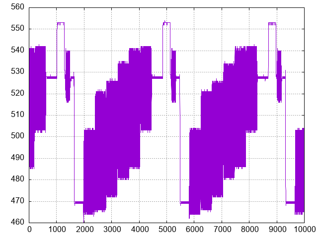
10x zoom display of 60 MS/s analog signal
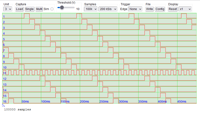
Logic analyser display
The controls are:
Single / repeat: control the data acquisition, with single or multiple captures
Sample count: number of samples required (max 100,000 for RP2040)
Sample rate: frequency of capture, up to 60 MHz for a Pico with a 120 MHz clock.
IP address: the address of the capture unit. This is printed out on the unit’s serial console at power-up.
Display: retrieve data from the unit without starting a new capture cycle.
Analogue/digital: select the number of logic analyser lines to display (8 or 16) or select the analog sensitivity (0.1, 0.2, 0.5 or 1.0 volts per division).
Zoom: Select the current zoom level; the trace can be dragged left or right to the required position.
The display code is in the ‘test’ directory on github here.
Alternative client software
An easy way to upload the data for further processing is to use WGET, e.g.
wget http://192.168.1.2/data.bin
This returns a file containing 16-bit binary data. Then the data can, for example, be plotted using GNUPlot:
gnuplot -e "set term png; set output 'data.png'; set grid; unset key; plot 'data.bin' binary array=10000 format='%uword' with lines;"
GNUplot of analog data
Copyright (c) Jeremy P Bentham 2024. Please credit this blog if you use the information or software in it.
A Web camera is quite a demanding application, since it requires a continuous stream of data to be sent over the network at high speed. The data volume is determined by the image size, and the compression method; the raw data for a single VGA-size (640 x 480 pixel) image is over 600K bytes, so some compression is desirable. Some cameras have built-in JPEG compression, which can compress the VGA image down to roughly 30K bytes, and it is possible to send a stream of still images to the browser, which will display them as if they came from a video-format file. This approach (known as motion-JPEG, or MJPEG) has a disadvantage in terms of inter-frame compression; since each frame is compressed in isolation, the compressor can’t reduce the filesize by taking advantage of any similarities between adjacent frames, as is done in protocols such as MPEG. However, MJPEG has the great advantage of simplicity, which makes it suitable for this demonstration.
Camera
The standard cameras for the full-size Raspberry Pi boards have a CSI (Camera Serial Interface) conforming to the specification issued by the MIPI (Mobile Industry Processor Interface) alliance. This high-speed connection is unsuitable for use with the Pico, we need something with a slower-speed SPI (Serial Peripheral Interface), and JPEG compression ability.
The camera I used is the 2 megapixel Arducam, which is uses the OV2640 sensor, combined with an image processing chip. It has I2C and SPI interfaces; the former is primarily for configuring the sensor, with the latter being for data transfer. Sadly the maximum SPI frequency is specified as 8 MHz, which compares unfavourably with the 60 MHz SPI we are using to communicate with the network.
The sensors require a large number of i2c register settings in order to function correctly. These are just ‘magic numbers’ copied across from the Arducam source code. The last block of values specify the sensor resolution, which is set at compile-time. The options are 320 x 240 (QVGA) 640 x 480 (VGA) 1024 x 768 (XGA) 1600 x 1200 (UXGA), e.g.
A single frame is captured by writing to a few registers, then waiting for the camera to signal that the capture (and JPEG compression) is complete. The size of the image varies from shot to shot, so it is necessary to read some register values to determine the actual image size. In reality, the camera has a tendency to round up the size, and pad the end of the image with some nulls, but this doesn’t seem to be a problem when displaying the image.
// Read single camera frame
int cam_capture_single(void)
{
    int tries = 1000, ret=0, n=0;

    cam_write_reg(4, 0x01);
    cam_write_reg(4, 0x02);
    while ((cam_read_reg(0x41) & 0x08) == 0 && tries)
    {
        usdelay(100);
        tries--;
    }
    if (tries)
        n = cam_read_fifo_len();
    if (n > 0 && n <= sizeof(cam_data))
    {
        cam_select();
        spi_read_blocking(CAM_SPI, 0x3c, cam_data, 1);
        spi_read_blocking(CAM_SPI, 0x3c, cam_data, n);
        cam_deselect();
        ret = n;
    }
    return (ret);
}
Reading the picture from the camera just requires the reading of a single dummy byte, then the whole block that represents the image; it is a complete JFIF-format picture, so no further processing needs to be done. If the browser has requested a single still image, we just send the whole block as-is to the client, with an HTTP header specifying “Content-Type: image/jpeg”
The following image was captured by the camera at 640 x 480 resolution:
MJPEG video
As previously mentioned, the Web server can stream video to the browser, in the form of a continuous flow of JPEG images. The requires a few special steps:
In the response header, the server defines the content-type as “multipart/x-mixed-replace”
To enable the browser to detect when one image ends, and another starts, we need a unique marker. This can be anything that isn’t likely to occur in the data stream; I’ve specified “boundary=mjpeg_boundary”
Before each image, the boundary marker must be sent, followed by the content-type (“image/jpeg”) and a blank line to mark the end of the header.
Timing
The timing will be quite variable, since it depends on the image complexity and network configuration, but here are the results of some measurements when fetching a single JPEG image over a small local network, using binary (not base64) mode:
Resolution (pixels)
Image capture time (ms)
Image size (kbyte)
TCP transfer time (ms)
TCP speed (kbyte/s)
320 x 240
153
10.2
4.4
2310
640 x 480
292
25.6
10.9
2350
1024 x 768
321
49.1
21.5
2285
1600 x 1200
420
97.3
42.4
2292
Web camera timings
The webcam code triggers an image capture, then after the data has been fetched into the CPU RAM buffer, it is sent to the network stack for transmission. There would be some improvement in the timings if the next image were fetched while the current image is being transmitted, however the improvement will be quite small, since the overall time is dominated by the time taken for the camera to capture and compress the image.
Using the Web camera
There is only one setting at the top of camera/cam_2640.h, namely the horizontal resolution:
It is important to note that a new image capture is triggered every time the Web page is accessed, so any attempt to simultaneously access the pages from more than one browser will fail. To allow simultaneous access by multiple clients, a double-buffering scheme needs to be implemented.
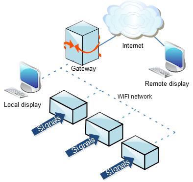
This is the third part of a 3-part blog post describing a low-cost WiFi-based logic analyser, that can be used for monitoring equipment in remote or hazardous locations. Part 1 described the hardware, part 2 the unit firmware, now this post describes the Web interface that controls the logic analyser units, and displays the captured data, also a Python class that can be used to remote-control the units for data analysis.
In a previous post, I experimented with shader hardware (via WebGL) for quickly displaying the logic analyser traces in a Web page. Whilst this technique can provide really fast display updates, there were some browser compatibility problems, and also a pure-javascript version proved to be fast enough, given that the main constraint is the time taken to transfer the data over the network.
So the current solution just used HTML and Javascript, with no hardware acceleration.
Network topology
REMLA network topology
In part 2, I described how the analyser units return data in response to Web page requests; the status information is in the form of a JSON string, and the sample data is Base64 encoded. So each unit has a built-in Web server, and it is tempting to load the HTML display files onto them. However, I chose not to do that, for the following reasons:
The analyser units use microcontrollers with finite resources, and not much spare storage space.
Every time the display software is updated, it would have to be loaded onto all the units individually.
It is easier to keep a single central server up-to-date with all the necessary security & access control measures.
So I’m assuming that there is a Web server somewhere on the system that serves the display file, and any necessary library files. This is a bit inconvenient for development, so when debugging I run a Web server on my development PC, for example using Python 3:
python -m http.server 8000
This launches a server on port 8000; if the display file is in a subdirectory ‘test’, its URL would look like:
http://127.0.0.1:8000/test/remla.html
There is also a question how the display program knows the addresses of the units, so it can access the right one. I had intended to use Multicast DNS (MDNS) for this purpose, but it proved to be a bit unreliable, so I assigned static IP addresses to the units instead.
Data display
The waveforms are drawn as vectors (as opposed to bitmaps), so the display can be re-sized to suit any size of screen. There are two basic drawing methods that can be used: an HTML canvas, or SVG (Scalable Vector Graphics). After some experimentation, I adopted the former, as it seemed to be a more flexible solution; the canvas is just an area of the screen that responds to simple line- and text-drawing commands, for example to draw & label the display grid:
var ctx1 = document.getElementById("canvas1").getContext("2d");
drawGrid(ctx1);

// Draw grid in display area
function drawGrid(ctx) {
  var w=ctx.canvas.clientWidth, h=ctx.canvas.clientHeight;
  var dw = w/xdivisions, dh=h/ydivisions;
  ctx.fillStyle = grid_bg;
  ctx.fillRect(0, 0, w, h);
  ctx.lineWidth = 1;
  ctx.strokeStyle = grid_fg;
  ctx.strokeRect(0, 1, w-1, h-1);
  ctx.beginPath();
  for (var n=0; n<xdivisions; n++) {
    var x = n*dw;
    ctx.moveTo(x, 0);
    ctx.lineTo(x, h);
    ctx.fillStyle = 'blue';
    if (n)
        drawXLabel(ctx, x, h-5);
    }
    for (var n=0; n<ydivisions; n++) {
      var y = n*dh;
      ctx.moveTo(0, y);
      ctx.lineTo(w, y);
    }
    ctx.stroke();
  }
Drawing the logic traces uses a similar method; begin a path, add line drawing commands to it, then invoke the stroke method.
Controls
The various control buttons and list boxes need to be part of a form, to simplify the process of sending their values to the analyser unit. So they are implemented as pure HTML:
To update the parameters on the unit, they are gathered from the form, and sent along with an optional command, e.g. cmd=1 to start a capture.
// Get form parameters
function formParams(cmd) {
  var formdata = new FormData(document.getElementById("captureForm"));
  var params = [];
  for (var entry of formdata.entries()) {
    params.push(entry[0]+ '=' + entry[1]);
  }
  if (cmd != null)
    params.push("cmd=" + cmd);
  return params;
}

// Get status from unit, optionally send command
function get_status(cmd=null) {
  http_request = new XMLHttpRequest();
  http_request.addEventListener("load", status_handler);
  http_request.addEventListener("error", status_fail);
  http_request.addEventListener("timeout", status_fail);
  var params = formParams(cmd), statusfile=remote_ip()+'/'+statusname;
  http_request.open( "GET", statusfile + "?" + encodeURI(params.join("&")));
  http_request.timeout = 2000;
  http_request.send();
}
The result of this HTTP request is handled by callbacks, for example if the request fails, there is a retry mechanism:
// Handle failure to fetch status page
function status_fail(e) {
  var evt = e || event;
  evt.preventDefault();
  if (retry_count < RETRIES) {
    addStatus(retry_count ? "." : " RETRYING")
    get_status();
    retry_count++;
  }
  else {
    doStop();
    redraw(ctx1);
  }
}
This mechanism was found to be necessary since very occasionally the remote unit fails to respond, for no apparent reason; if there is a real reason (e.g. it has been powered down) then the transfer is halted after 3 attempts.
If the status information has been returned OK, then a suitable action is taken; if a capture has been triggered, and the status page indicates that the capture is complete, then the data is fetched:
// Decode status response
function status_handler(e) {
  var evt = e || event;
  var remote_status = JSON.parse(evt.target.responseText);
  var state = remote_status.state;
  if (state != last_state) {
    dispStatus(state_strs[state]);
    last_state = state;
  }
  addStatus(".");
  if (state==STATE_IDLE || state==STATE_PRELOAD || state==STATE_PRETRIG || state==STATE_POSTTRIG) {
    repeat_timer = setTimeout(get_status, 500);
  }
  else if (remote_status.state == STATE_READY) {
    loadData();
  }
  else {
    doStop();
  }
}
Fetching data
Fetching the data is similar to fetching the status page, since it is a text file containing base64-encoded bytes. The callback converts the text into bytes, then pairs of bytes into an array of numeric values:
// Read captured data (display is done by callback)
function loadData() {
  dispStatus("Reading from " + remote_ip());
  http_request = new XMLHttpRequest();
  http_request.addEventListener("progress", capfile_progress_handler);
  http_request.addEventListener( "load", capfile_load_handler);
  var params = formParams(), capfile=remote_ip()+'/'+capname;
  http_request.open( "GET", capfile + "?" + encodeURI(params.join("&")));
  http_request.send();
}

// Display data (from callback event)
function capfile_load_handler(event) {
  sampledata = getData(event.target.responseText);
  doZoomReset();
  if (command == CMD_MULTI)
    window.requestAnimationFrame(doStart);
  else
    doStop();
}

// Get data from HTTP response
function getData(resp) {
  var d = resp.replaceAll("\n", "");
  return strbin16(atob(d));
}

// Convert string of 16-bit values to binary array
function strbin16(s) {
  var vals = [];
  for (var n=0; n<s.length;) {
    var v = s.charCodeAt(n++);
    vals.push(v | s.charCodeAt(n++) << 8);
  }
  return vals;
}
It is probable that this process could be streamlined somewhat, but currently the main speed restriction is the transfer of data from the ESP to the PC over the wireless network, so improving the byte-decoder wouldn’t give a noticeable speed improvement.
Saving the data
There needs to be some way of saving the sample data for further analysis; as it happens, the initial users of the system were already using the open-source Sigrok Pulseview utility for capturing data from small USB pods, so it was decided to save the data in the Sigrok file format.
This a basically a zipfile, with 3 components:
Metadata, identifying the channels, sample rate, etc.
Version, giving the file format version (currently 2)
Logic file, containing the binary data
The metadata format is quite easy to replicate, e.g.
[global]
sigrok version=0.5.1

[device 1]
capturefile=logic-1
total probes=16
samplerate=5 MHz
total analog=0
probe1=D1
probe2=D2
probe3=D3
..and so on until..
probe16=D16
unitsize=2
The dummy labels D1, D2 etc. are normally replaced with meaningful descriptions of the signals, followed by the unitsize parameter which gives the byte-width of the data, and marks the end of the labels.
The JSZip library is used to zip the various components together in a single file with the ‘sr’ extension:
function write_srdata(fname) {
  var meta = encodeMeta(), zip = new JSZip();
  var samps = new Uint16Array(sampledata);
  zip.file("metadata", meta);
  zip.file("version", "2");
  zip.file("logic-1-1", samps.buffer);
  zip.generateAsync({type:"blob", compression:"DEFLATE"})
  .then(function(content) {
    writeFile(fname, "application/zip", content);
  });
}

// Encode Sigrok metadata
function encodeMeta() {
  var meta=[], rate=elem("xrate").value + " Hz";
  for (var key in sr_dict) {
    var val = key=="samplerate" ? rate : sr_dict[key];
    meta.push(val[0]=='[' ? ((meta.length ? "\n" : "") + val) : key+'='+val);
  }
  for (var n=0; n<nchans; n++) {
    meta.push("probe"+(n+1) + "=" + (probes.length?probes[n]:n+1));
  }
  meta.push("unitsize=2");
  return meta.join("\n");
}
Configuration
So far, the only way the units can be configured is by using the browser controls, to set the sample rate, number of samples, threshold etc. Whilst this might be acceptable for a portable system, a semi-permanent installation needs some way of storing the configuration, including the naming of input channels on the display. Since there is a central Web server for the display files, can’t this also be used to store configuration files? The answer is ‘yes’, but there is then a question how these files can be modified in a browser-friendly way.
This is a bit difficult, since there are numerous security protections for the files on a server, to make sure they can’t be modified by a Web client. However, there is an extension to the HTTP protocol known as WebDAV (Web Distributed Authoring and Versioning), which does provide a mechanism for writing to files. Basically you need a general-purpose Web server that can be configured to support Web DAV (such as lighttpd, see this page), or alternatively a special-purpose server, such as wsgidav (see this page).
Assuming you already have a working lighttpd server, the additional configuration file may look something like this, with some_path, dav_username and dav_password being customised for your installation:
Again, this will need to be customised for your environment, and you also need to be mindful that the configurations I’ve shown for lighttpd and wsgidav are quite insecure, for example the password isn’t encrypted, so it can easily be captured by anyone snooping on network traffic.
Configuration Web page
I created a simple Web page to handle the configuration, with list boxes for most options, and text boxes to allow the input channels to be named.
At the bottom of the page there are buttons to submit the new configuration to the server, and exit back to the waveform display page.
The key Javascript function to save the configuration on the server uses the ‘davclient’ library, and is quite simple, but it does need to know the host IP address and port number to receive the data. This code attempts to fetch that information using the DOM Location object:
// Save the config file
function saveConfig() {
  var fname = CONFIG_UNIT.replace('$', String(unitNum()));
  var ip = location.host.split(':')
  var host = ip[0], port = ip[1];
  port = !port ? 80 : parseInt(port);
  var davclient = new davlib.DavClient();
  davclient.initialize(host, port, 'http', DAVUSER, DAVPASS);
  davclient.PUT(fname, JSON.stringify(getFormData()), saveHandler)
 }
For simplicity, the DAV username and password are stored as plain text in the Javascript, which means that anyone viewing the page source can see what they are. This makes the server completely insecure, and must be improved.
Python interface
Although some data analysis can be done in Javascript, it is much more convenient to use Python and its numerical library numpy. I have written a Python class EdlaUnit that provides an API for remote control and data analysis, and a program edla_sweep that demonstrates this functionality.
It repeatedly captures a data block, whilst stepping up the threshold voltage. Then for each block, the number of transitions for each channel is counted and displayed.
import edla_utils as edla, base64, numpy as np

edla.verbose_mode(False)
unit = edla.EdlaUnit(1, "192.168.8")
unit.set_sample_rate(10000)
unit.set_sample_count(10000)

MIN_V, MAX_V, STEP_V = 0, 50, 5

def get_data():
    ok = False
    data = None
    status = unit.fetch_status()
    if status:
        ok = unit.do_capture()
    else:
        print("Can't fetch status from %s" % unit.status_url)
    if ok:
        data = unit.do_load()
    if data == None:
        print("Can't load data")
    return data

for v in range(MIN_V, MAX_V, STEP_V):
    unit.set_threshold(v)
    d = get_data()
    byts = base64.b64decode(d)
    samps = np.frombuffer(byts, dtype=np.uint16)
    diffs = np.diff(samps)
    edges = np.where(diffs != 0)[0]
    totals = np.zeros(16, dtype=int)
    for edge in edges:
        bits = samps[edge] ^ samps[edge+1]
        for n in range(0, 15):
            if bits & (1<<n):
                totals[n] += 1
    s = "%4u," % v
    s += ",".join([("%4u" % val) for val in totals])
    print(s)
The idea is to give a quick overview of the logic levels the analyser is seeing, to make sure they are within reasonable bounds. An example output is:
The absolute count isn’t necessarily very important, since it will vary depending on the signal that is being monitored. What is interesting is the way it changes as the threshold voltage increases. If the number dramatically increases as the ‘1’ logic voltage is approached, one might suspect that there is a noise problem, causing spurious edges. Conversely, if the value declines rapidly before the ‘1’ voltage is reached, the logic level is probably too low.
There is a tendency to assume that all logic signals are a perfect ‘1’ or ‘0’, with nothing in between; this technique allows you to look beyond that, and check whether your signals really are that perfect – and of course you can use the power of Python and numpy to do other analytical tests, or protocol decoding, specific to the signals being monitored.
—
Part 1 of this project looked at the hardware, part 2 the ESP32 firmware. The source files are on Github.
Copyright (c) Jeremy P Bentham 2022. Please credit this blog if you use the information or software in it.
This is the second part of a 3-part blog post describing a low-cost WiFi-based logic analyser, that can be used for monitoring equipment in remote or hazardous locations. Part 1 described the hardware, this post now describes the firmware within the logic analyser unit.
Development environment
There are two main development environments for the ESP32 processor; ESP-IDF and Arduino-compatible. The former is much more comprehensive, but a lot of those features aren’t needed, so to save time, I have used the latter.
There are two ways of developing Arduino code; using the original Arduino IDE, or using Microsoft Visual Studio Code (VS Code) with a build system called PlatformIO. I originally tried to support both, but found the Arduino IDE too restrictive, so opted for VS Code and PlatformIO.
Then it is just necessary to open a directory containing the project files, and after a suitable pause while the necessary files are downloaded, the source files can be compiled, and the resulting binary downloaded onto the ESP32 module.
Visual Studio Code IDE
The code has two main areas: driving the custom hardware that captures the samples, and the network interface.
Hardware driver
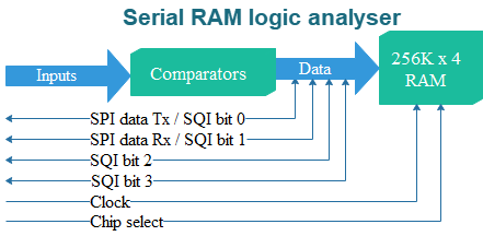
As described in the previous post, the main hardware elements driven by the CPU are:
16-bit data bus for the RAM chips and the comparator outputs
Clock & chip select for RAM chips
SPI interface for the DAC that sets the threshold
Data bus
The sample memory consists of four 23LC1024 serial RAM chips, each storing 1 Mbit in quad-SPI (4-bit) mode. They are arranged to form a 16-bit data bus; it would be really convenient if this could be assigned to 16 consecutive I/O bits on the CPU, but the ESP32 hardware does not permit this. The assignment is:
There is an obvious requirement to handle the data bus as a single 16-bit value within the code, so it is necessary to provide functions that convert that 16-bit data into a 32-bit value to be fed to the I/O pins, and vice-versa, and it’d be helpful if this was done in an easy-to-understand manner, to simplify any changes when a new CPU is used that has a different pin assignment.
After having tried the usual mess of shift-and-mask operations, I hit upon the idea of creating a bitfield for each group of consecutive GPIO pins, and a matching bitfield for the same group in the 16-bit word; then it is only necessary to equate each field to its partner, to produce the required conversion.
// Data bus pin definitions
// z-variables are unused pins
typedef struct {
    uint32_t z1:4, d0_1:2, z2:6, d2_9:8, z3:1, d10_12:3, z4:1, d13_15:3;
} BUSPINS;
typedef union {
    uint32_t val;
    BUSPINS pins;
} BUSPINVAL;

// Matching elements in 16-bit word
typedef struct {
    uint32_t d0_1:2, d2_9:8, d10_12:3, d13_15:3;
} BUSWORD;
typedef union {
    uint16_t val;
    BUSWORD bits;
} BUSWORDVAL;

// Return 32-bit bus I/O value, given 16-bit word
inline uint32_t word_busval(uint16_t val) {
    BUSWORDVAL w = { .val = val };
    BUSPINVAL  p = { .pins = { 0, w.bits.d0_1,   0, w.bits.d2_9,
                               0, w.bits.d10_12, 0, w.bits.d13_15 } };
    return (p.val);
}

// Return 16-bit word, given 32-bit bus I/O value
inline uint16_t bus_wordval(uint32_t val) {
    BUSPINVAL  p = { .val = val };
    BUSWORDVAL w = { .bits = { p.pins.d0_1, p.pins.d2_9,
                               p.pins.d10_12, p.pins.d13_15 } };
    return (w.val);
}
An additional complication is that the 16-bit value is going to 4 RAM chips, and each chip needs to receive the same command, and the bit-pattern of that command changes depending on whether the chip is in SPI or quad-SPI (QSPI, also known as SQI) mode. So the command to send a command to all 4 RAM chips in SPI mode is:
#define RAM_SPI_DOUT    1
#define MSK_SPI_DOUT    (1 << RAM_SPI_DIN)
#define ALL_RAM_WORD(b) ((b) | (b)<<4 | (b)<<8 | (b)<<12)
uint32_t spi_dout_pins = word_busval(ALL_RAM_WORD(MSK_SPI_DOUT));

// Send byte command to all RAMs using SPI
// Toggles SPI clock at around 7 MHz
void bus_send_spi_cmd(byte *cmd, int len) {
    GPIO.out_w1ts = spi_hold_pins;
    while (len--) {
        byte b = *cmd++;
        for (int n = 0; n < 8; n++) {
            if (b & 0x80) GPIO.out_w1ts = spi_dout_pins;
            else GPIO.out_w1tc = spi_dout_pins;
            SET_SCK;
            b <<= 1;
            CLR_SCK;
        }
    }
}
I have used a ‘bit-bashing’ technique (i.e. manually driving the I/O pins high or low) since I’m emulating 4 SPI transfers in parallel, and as you can see from the comment, the end-result is reasonably fast.
When the RAMS are in QSPI mode, instead of doing eight single-bit transfers, we must do two four-bit transfers:
// Send a single command to all RAMs using QSPI
void bus_send_qspi_cmd(byte *cmd, int len) {
    while (len--) {
        uint32_t b1=*cmd>>4, b2=*cmd&15;
        uint32_t val=word_busval(ALL_RAM_WORD(b1));
        gpio_out_bus(val);
        SET_SCK;
        val = word_busval(ALL_RAM_WORD(b2));
        CLR_SCK;
        gpio_out_bus(val);
        SET_SCK;
        cmd++;
        CLR_SCK;
    }
}
The above code assumes that the appropriate I/O pin-directions (input or output) have been set, but that too depends on which mode the RAMs are in; for SPI each RAM chip has 2 data inputs (DIN and HOLD) and 1 output (DOUT), whilst in QSPI mode all 4 RAM data pins are inputs or outputs depending on whether the RAM is being written to, or read from.
There are 4 commands that the software sends to the RAM chips, each is a single byte:
0x38: enter quad-SPI (QSPI) mode
0xff: leave QPSI mode, enter SPI mode
0x02: write data
0x03: read data
The read & write commands are followed by a 3-byte address value, that dictates the starting-point for the transfer. So if the RAMs are already in QSPI mode, the sequence for capturing samples is:
Set bus pins as outputs, so bus is controlled by CPU
Assert RAM chip select
Send command byte, with a value of 2 (write)
Send 3 address bytes (all zero when starting data capture)
Set bus pins as inputs, so bus is controlled by comparators
Start RAM clock
When capture is complete, stop RAM clock
Negate RAM chip select
The steps for recovering the captured data are:
Set bus pins as outputs, so bus is controlled by CPU
Assert RAM chip select
Send command byte, with a value of 3 (read)
Send 3 address bytes
Set bus pins as inputs, so bus is controlled by the RAM chips
Toggle clock line, and read data from the 16-bit bus
When readout is complete, negate RAM chip select
RAM clock and chip select
When the CPU is directly accessing the RAM chips (to send commands, or read back data samples) it is most convenient to ‘bit-bash’ the clock and I/O signals, as described above. It is possible that incoming interrupts can cause temporary pauses in the clock transitions, but this doesn’t matter: the RAM chips use ‘static’ memory, which won’t change its state even if there is a very long pause in a transfer cycle.
However, when capturing data, it is very important that the RAMs receive a steady clock at the required sample rate, with no interruptions. This is easily achieved on the ESP32 by using the LED PWM peripheral:
In addition, the CPU must count the number of pulses that have been output, so that it knows which memory address is currently being written – there is no way to interrogate the RAM chip to establish its current address value. Surprisingly, the ESP32 doesn’t have a general-purpose 32-bit counter, so we have to use the 16-bit pulse-count peripheral instead, and detect overflows in order to produce a 32-bit value.
When writing this code, I came across some strange features of the PCNT interrupt, such as multiple interrupts for a single event, and misleading values when reading the count value inside the interrupt handler, so be careful when doing any modifications.
The pulse count does not equal the RAM address; is the RAM address multiplied by 2. This is because it takes two 4-bit write cycles to create one byte in RAM (bits 4-7, then 0-3), so the memory chip increments its RAM address once for every 2 samples.
All the RAMs share a single clock line and chip select; the select line is driven low at the start of a command, and must remain low for the duration of the command and data transfer; when it goes high, the transfer is terminated.
Setting threshold value
The comparators compare the incoming signal with a threshold value, to determine if the value is 1 or 0 (above or below threshold). The threshold is derived from a digital-to-analog converter (DAC), the part I’ve chosen is the Microchip MCP4921; it was necessary to use a part with an SPI interface, since there is only 1 spare output pin, which serves as the chip select for this device; the clock and data pins are shared with the RAM chips.
This means that the DAC control code can use the same drivers as the RAM chips by negating the RAM chip select, and asserting the DAC chip select:
Triggering is achieved by using the ESP32 pin-change interrupt, as this can capture quite a narrow pulses. There will be a delay before the interrupt is serviced, which means that we don’t get an accurate indication of which sample caused the trigger, but that isn’t a problem in practice.
int trigchan, trigflag;

// Handler for trigger interrupt
void IRAM_ATTR trig_handler(void) {
    if (!trigflag) {
        trigsamp = pcnt_val32();
        trigflag = 1;
    }
}

// Enable or disable the trigger interrupt for channels 1 to 16
void set_trig(bool en) {
    int chan=server_args[ARG_TRIGCHAN].val, mode=server_args[ARG_TRIGMODE].val;
    if (trigchan) {
        detachInterrupt(busbit_pin(trigchan-1));
        trigchan = 0;
    }
    if (en && chan && mode) {
        attachInterrupt(busbit_pin(chan-1), trig_handler,
            mode==TRIG_FALLING ? FALLING : RISING);
        trigchan = chan;
    }
    trigflag = 0;
}
This interrupt handler sets a flag, that is actioned by the main state machine. There is a ‘trig_pos’ parameter that sets how many tenths of the data should be displayed prior to triggering; it is normally set to 1, which means that (approximately) 1 tenth will be displayed before the trigger, and 9 tenths after.
It is possible that there may be a considerable delay before the trigger event is encountered. In this case, the unit continues to capture samples, and the RAM address counter will wrap around every time it reaches the maximum value. This means that the pre-trigger data won’t necessarily begin at address zero; the firmware has to fetch the trigger RAM address, then jump backwards to find the start of the data.
State machine
This handles the whole capture process. There are 6 states:
Idle: no data, and not capturing data
Ready: data has been captured, ready to be uploaded
Preload: capturing data, before looking for trigger
PreTrig: capturing data, looking for trigger
PostTrig: capturing data after trigger
Upload: transferring data over the network
The Preload state is needed to ensure there is some data prior to the trigger. If triggering is disabled, then as soon as the capture is started, the software goes directly to the PostTrig state, checking the sample count to detect when it is greater than the requested number.
// Check progress of capture, return non-zero if complete
bool web_check_cap(void) {
    uint32_t nsamp = pcnt_val32(), xsamp = server_args[ARG_XSAMP].val;
    uint32_t presamp = (xsamp/10) * server_args[ARG_TRIGPOS].val;
    STATE_VALS state = (STATE_VALS)server_args[ARG_STATE].val;
    server_args[ARG_NSAMP].val = nsamp;
    if (state == STATE_PRELOAD) {
        if (nsamp > presamp)
            set_state(STATE_PRETRIG);
    }
    else if (state == STATE_PRETRIG) {
        if (trigflag) {
            startsamp = trigsamp - presamp;
            set_state(STATE_POSTTRIG);
        }
    }
    else if (state == STATE_POSTTRIG) {
        if (nsamp-startsamp > xsamp) {
            cap_end();
            set_state(STATE_READY);
            return(true);
        }
    }
    return (false);
}
Network interface
A detailed description of network operation will be found in part 3 of this project; for now, it is sufficient to say that the unit acts as a wireless client, connecting to a pre-defined WiFi access point; it has a simple Web server with all requests & responses using HTTP.
Wireless connection
The first step is to join a wireless network, using a predefined network name (‘SSID’) and password. The code must also try to re-establish the link to he Access Point if the connection fails, so there is a polling function that checks for connectivity.
// Begin WiFi connection
void net_start(void) {
    DEBUG.print("Connecting to ");
    DEBUG.println(ssid);
    WiFi.begin(ssid, password);
    WiFi.setSleep(false);
}

// Check network is connected
bool net_check(void) {
    static int lastat=0;
    int stat = WiFi.status();
    if (stat != lastat) {
        if (stat<=WL_DISCONNECTED) {
            DEBUG. printf("WiFi status: %s\r\n", wifi_states[stat]);
            lastat = stat;
        }
        if (stat == WL_DISCONNECTED)
            WiFi.reconnect();
    }
    return(stat == WL_CONNECTED);
}
Web server
The Web pages are very simple and only contain data; the HTML layout and Javascript code to display the data is fetched from a different server.
The server is initialised with callbacks for three pages:
#define STATUS_PAGENAME "/status.txt"
#define DATA_PAGENAME   "/data.txt"
#define HTTP_PORT       80

WebServer server(HTTP_PORT);

// Check if WiFi & Web server is ready
bool net_ready(void) {
    bool ok = (WiFi.status() == WL_CONNECTED);
    if (ok) {
        DEBUG.print("Connected, IP ");
        DEBUG.println(WiFi.localIP());
        server.enableCORS();
        server.on("/", web_root_page);
        server.on(STATUS_PAGENAME, web_status_page);
        server.on(DATA_PAGENAME, web_data_page);
        server.onNotFound(web_notfound);
        DEBUG.print("HTTP server on port ");
        DEBUG.println(HTTP_PORT);
        delay(100);
    }
    return (ok);
}
The root page returns a simple text string, and is mainly used to check that the Web server is functioning:
This indicates that 10000 samples were requested at 100 KS/s, 10010 were actually collected, using a threshold of 10 volts. The ‘state’ value of 1 indicates that data collection is complete, and the data is ready to be uploaded.
The individual arguments are stored in an array of structures, which is converted into the JSON string:
typedef struct {
    char name[16];
    int val;
} SERVER_ARG;

SERVER_ARG server_args[] = {
    {"state",       STATE_IDLE},
    {"nsamp",       0},
    {"xsamp",       10000},
    {"xrate",       100000},
    {"thresh",      THRESH_DEFAULT},
    {"trig_chan",   0},
    {"trig_mode",   0},
    {"trig_pos",    1},
    {""}
};

// Return server status as json string
int web_json_status(char *buff, int maxlen) {
    SERVER_ARG *arg = server_args;
    int n=sprintf(buff, "{");
    while (arg->name[0] && n<maxlen-20) {
        n += sprintf(&buff[n], "%s\"%s\":%d", n>2?",":"", arg->name, arg->val);
        arg++;
    }
    return(n += sprintf(&buff[n], "}"));
}
The HTTP request for the status page can also include a query string with parameters that reflect the values the user has entered in a Web form. If a ‘cmd’ parameter is included, it is interpreted as a command; the following query includes ‘cmd=1’, which starts a new capture:
GET /status.txt?unit=1&thresh=10&xsamp=10000&xrate=100000&trig_mode=0&trig_chan=0&zoom=1&cmd=1
The software matches the parameters with those in the server_args array, and stores the values in that array; unmatched parameters (such as the zoom level) are ignored.
// Return status Web page
void web_status_page(void) {
    web_set_args();
    web_do_command();
    web_json_status((char *)txbuff, TXBUFF_LEN);
    server.sendHeader(HEADER_NOCACHE);
    server.setContentLength(CONTENT_LENGTH_UNKNOWN);
    server.send(200, "application/json");
    server.sendContent((char *)txbuff);
    server.sendContent("");
}

// Get command from incoming Web request
int web_get_cmd(void) {
    for (int i=0; i<server.args(); i++) {
        if (!strcmp(server.argName(i).c_str(), "cmd"))
            return(atoi(server.arg(i).c_str()));
    }
    return(0);
}

// Get arguments from incoming Web request
void web_set_args(void) {
    for (int i=0; i<server.args(); i++) {
        int val = atoi(server.arg(i).c_str());
        web_set_arg(server.argName(i).c_str(), val);
    }
}
Data transfer
The captured data is transferred using an HTTP GET request to the page data.txt. The binary data is encoded using the base64 method, which converts 3 bytes into 4 ASCII characters, so it can be sent as a text block. There is insufficient RAM in the ESP32 to store the sample data, so it is transferred on-the-fly from the RAM chips to a network buffer.
// Return data Web page
void web_data_page(void) {
    web_set_args();
    web_do_command();
    server.sendHeader(HEADER_NOCACHE);
    server.setContentLength(CONTENT_LENGTH_UNKNOWN);
    server.send(200, "text/plain");
    cap_read_start(startsamp);
    int count=0, nsamp=server_args[ARG_XSAMP].val;
    size_t outlen = 0;
    while (count < nsamp) {
        size_t n = min(nsamp - count, TXBUFF_NSAMP);
        cap_read_block(txbuff, n);
        byte *enc = base64_encode((byte *)txbuff, n * 2, &outlen);
        count += n;
        server.sendContent((char *)enc);
        free(enc);
    }
    server.sendContent("");
    cap_read_end();
}
The ‘unknown’ content length means that the software can send an arbitrary number of text blocks, without having to specify the total length in advance. The transfer is terminated by calling sendContent with a null string.
Diagnostics
There is a single red LED, but due to pin constraints, it is shared with the RAM chip select. So it will always illuminate when the RAM is being accessed, but in addition:
Rapid flashing (5 Hz) if the unit is not connected to the WiFi network
Brief flash (100 ms every 2 seconds) when the unit is connected to the network.
Solid on when the unit is capturing data, and is waiting for a trigger, or until the required amount of data has been collected.
There is also the ESP32 USB interface that emulates a serial console at 115 Kbaud:
#define DEBUG_BAUD  115200
#define DEBUG       Serial      // Debug on USB serial link

DEBUG.begin(DEBUG_BAUD);

// 'print' 'println' and 'printf' functions are supported, e.g.
DEBUG.print("Connecting to ");
DEBUG.println(ssid);
To view the console display, you can use your favourite terminal emulator (e.g. TeraTerm on Windows) connected to the USB serial port, however you will have to break that connection every time you re-program the ESP32, since it is needed for re-flashing the firmware. The VS Code IDE does have its own terminal emulator, which generally auto-disconnects for re-programming, but I have had occasional problems with this feature, for reasons that are a bit unclear.
Modifications
There are a few compile-time options that need to be set before compiling the source code:
SW_VERSION (in main.cpp): a string indicating the current software version number
ssid & password (in esp32_web.cpp): must be changed to match your wireless network
THRESH_SCALE (in esp32_la.h): the scaling factor for the threshold value, that is used to program the DAC.
The threshold scaling will depend on the values of the attenuator resistors. The unit was originally designed for input voltages up to 50V, with a possible overload to 250V, so the input attenuation was 101 (100K series resistor, 1K shunt resistor). If using the unit with, say, 5 volt logic, then the series resistor will need to be much lower (and maybe the shunt resistance a bit higher) so the threshold scaling value will need to be adjusted accordingly. Since the threshold value sent from the browser is an integer value (currently 0 – 50) you might choose the redefine that value when working with lower voltages, for example represent 0 – 7 volts as a value of 0 – 70, in tenths of a volt. This change will need to be made in the firmware, and both Web interfaces.
An important note, when creating a new unit. Since I’m using all the available I/O pins on the ESP32, I’ve had to use GPIO12, even though this does (by default) determine the Flash voltage at startup.
To use the pin for I/O, it is essential that this behaviour is changed by modifying the parameters in the ESP32 one-time-programmable memory. This is done using the Python espefuse program that is provided in the IDE. To summarise the current settings, navigate to the directory containing that file, and execute:
python espefuse.py --port COM4 summary
..assuming the USB serial link is on Windows COM port 4. Then to modify the setting, execute:
This is the first post in a series describing a low-cost WiFi-based logic analyser, that can be used for monitoring equipment in remote or hazardous locations. For an overview of the project, see this post. The hardware specification is:
Digital inputs: 16 for each unit
Input threshold: programmable
Sample rate: up to 20 megasamples per second
Sample store: up to 250 kilosamples
Network interface: WiFi
Wireless networking is an essential component of this project, and at the time of writing, the most logical hardware choice is the Espressif ESP32, which is a microcontroller with up to 34 GPIO pins, an Xtensa dual-core 32-bit LX6 processor, and built-in WiFi.
Sample storage
There are ESP32 variants with differing amounts RAM & flash ROM, but currently the most common type is the ESP32-S2 with 320 KiB SRAM and 128 KiB ROM. A significant portion of this is taken up by the WiFi code, so there is insufficient RAM to store the required number of samples.
When using external memory for sample storage, the standard practice is to employ one or more RAM chips and an address counter that is fed from a constant clock that increments when a sample is stored.
Unfortunately, the 16 data lines plus 18 address lines make this arrangement quite bulky, even when implemented using surface-mount parts. One way of simplifying the circuit is to embed the logic within a programmable logic device, such as a Field-Programmable Gate Array (FPGA), but the programming & debugging of such a device can be quite complex.
Ideally, what we want is a RAM device that has a built-in address counter, that will auto-increment on each sample. Such devices do exist, they are known as ‘Serial SRAM’; they have a 1-bit, 2-bit or 4-bit clocked serial interface for sending commands and data. You may be familiar with 1-bit SPI (Serial Peripheral Interface), as it is used in a wide variety of devices, and the RAM chip is in this mode on startup. Less well-known are the 2-bit (SDI or DSPI) and 4-bit (SQI or QSPI) interfaces that use the same hardware lines unidirectionally; commands are sent to read or write data in these modes, and thereafter the RAM chip transfers the data with an auto-incrementing address counter that wraps around at the end of the RAM.
Each RAM chip handles 4 input channels, so 4 chips are needed for the 16-channel input.
The following steps are needed for data capture:
Send command to switch RAM from SPI to SQI mode
Send a ‘write’ command, with the desired starting address
Assert the chip select line, and start the clock signal.
When capture is complete, stop the clock signal
Negate chip select, which completes the ‘write’ command
Readback of the captured data is similar, except that a ‘read’ command is used.
Unfortunately there is no way to read back the address counter within the RAM chip, so to keep track of the sampling process, it is necessary to attach a pulse counter to the clock line; a counter/timer within the microcontroller can be used for this purpose.
Another issue is the fact that the RAM data lines serve two purposes; to receive data from the comparators, and commands from the CPU. Ideally the comparators would have an ‘enable’ pin to tri-state their outputs, but I couldn’t find a suitable device with this feature. Failing that, the conventional approach would be to use multiplexer chips to switch between the two data sources, but I’ve taken a much simpler approach, using resistors in the output of the comparators. When the CPU is in control, it just sets the data lines high or low as required, overriding the comparator outputs; when capturing data, the CPU sets its pins as inputs, so the comparators control the data going into the RAM, albeit with a small delay due to the 1K series resistance interacting with the circuit capacitance, but this hasn’t proved a problem in practice.
Triggering
An important feature of logic analysers is triggering; the ability to continuously capture data until a specific condition is met, carry on capturing for a specific number of samples after the trigger, then stop.
The logic to support this operation can be quite complex, and the addition of digital comparators (or their equivalent in programmable logic) would be a major complication. However, it is worth bearing in mind two things:
If there is a small time-delay between the trigger condition being detected, and the hardware reacting to the trigger, then it is no problem; if we are capturing tens of thousands of samples, a trigger delay of 10 or 20 samples is of no great concern.
The CPU is largely idle while data is being captured; it only has to respond to network requests, which are largely handled by the 2nd CPU in a dual-CPU device.
In common with most modern microcontrollers, the ESP32 has the ability to generate an interrupt on the state-change of any I/O pin, and this interrupt can be used for triggering, since it can capture very short pulses (under 50 nanoseconds). In theory it is possible to chain several edge-interrupts together, to give more complex triggering, but personally I’ve found a single edge-trigger to be sufficient for most purposes.
ESP32
The decision to use an ESP32 processor was largely driven by its built-in WiFi interface, and the ready availability of complete low-cost modules with a built-in antenna (or connector for an external antenna). The module used is the ESP32-S2-DevKitC with 38 pins, and an ESP32-WROOM-32D or -32E processor; take care not not to be confuse it with similar-looking modules.
This module has a few features that make it an excellent choice:
Fast dual-CPU architecture.
Easy-to-use C software development environment based on the VScode IDE, PlatformIO configuration, and the Arduino run-time environment.
A pin multiplexer that removes a lot of constraints as to which pins can be used for which internal functions
Simple PWM generator that can generate the required clock frequencies
Edge-detection interrupts on any I/O pin.
However, there are some less-than-ideal features:
Gaps in the I/O pin assignments, so it is impossible to assign 8 consecutive bits to form a single byte-wide input, or 16 consecutive bits to form a word-wide input.
Absence of a general-purpose 32-bit pulse counter; only 16 bits are available.
Usage of some I/O pins to specify boot-time settings.
Some GPIO pins are input-only.
These issues can be resolved in software, as will be described in the next blog post, but the final design does use all the input/output pins, with none spare, which forces some economies. For example, it is highly desirable to have a diagnostic LED controlled by the CPU, but there is no O/P pin to drive it, so it has been put on the RAM chip-select line, which slightly reduces the flexibility of the LED indications.
Analog inputs
Each analog input requires an attenuator to reduce the input voltage down to something manageable, and a comparator that compares the attenuated signal with a programmable reference voltage produced by a DAC (Digital-Analog Converter).
The attenuator is just a resistive potential divider; the resistors have been arranged in groups of 8, such that dual-in-line (DIL) plug-in resistor packs can be used in place of discrete resistors. This means that the board can handle very a wide range of input voltages by plugging in different resistor packs.
It proved quite difficult to find a comparator that is readily available, fast enough, and with a push-pull output (not open-drain). An early candidate was the MAX942, but this has back-to-back diodes between the inverting and non-inverting inputs, which would cause major problems if the voltage difference was sufficiently high to make them conduct. In the end, TS3022 devices in SO-8 packages were selected, and they perform really well; provision had been made for adding positive feedback to provide hysteresis (by adding resistors to the DIL-footprint through-holes), but in practice this has not been necessary.
Programming
The ESP32 module has a micro USB connector to provide power to the unit, and a programming interface. As a backup, the PCB also includes a JTAG programming interface, but this uses some of the data pins, so is only usable on a bare depopulated PCB.
The USB interface also emulates a serial console, that is compatible with standard PC terminal emulators; the ESP32 firmware makes extensive use of this for diagnostic reporting.
PCB design
Assembled logic analyser unit
The circuit diagram, PCB manufacturing files (Gerbers) and parts list are in the project repository; do check the README file for the latest information.
The PCB has dual-footprints (DIL & SO-8) for the memory chips and the comparators. I have used DIL sockets for the RAM chips so they can be upgraded at a future date, but as mentioned above, none of the DIL-packaged comparators were suitable, so surface-mount TS3022 parts were used – they have a relatively generous pin spacing (1.27 mm) so shouldn’t be difficult for anyone to assemble who has reasonable soldering skills.
The photo above shows socketed resistor packs for the input attenuators; if using these (as opposed to individual resistors) make sure you buy the type with 8 individual resistors, not commoned.
The ESP32 module requires two 19-way sockets with square pins; I had to use 20-pin parts, with one pin cut off. To help with hardware diagnostics, I have included convenient 2.54 mm pitch headers for the RAM clock, chip select and data lines. These only need to be populated if you are using a logic analyser to trace the board’s operation, or if you wish to remove the ESP32 module and drive the board from some other CPU.
Power (5 volts, with a current capacity of at least 250 mA) is either applied on the USB connector, or on P14, in which case there needs to be an on/off switch connected to the terminals of P7, or those pins must be bonded across. The module is programmed over USB; do not use the JTAG interface unless the board is de-populated.
Part 2 of this project looks at the ESP32 firmware, part 3 the Web interface and Python API. The circuit diagram and PCB files are on Github.
Copyright (c) Jeremy P Bentham 2022. Please credit this blog if you use the information or software in it.
There are plenty of low-cost logic analysers but they all share a common characteristic; a USB link is used to transfer the data into a PC for analysis.
If the equipment is in a safe & comfortable office environment, then this isn’t a problem, but in many cases it is operating in an distant, inaccessible or hostile location, so remote monitoring is desirable. If the analyser unit is small and low-cost, it can remain attached on a semi-permanent basis, enabling long-term monitoring & diagnosis of remote equipment
The initial specification of the logic analyser unit is
Digital inputs: 16 for each unit
Input threshold: programmable
Sample rate: up to 20 megasamples per second
Sample store: up to 250 kilosamples
Network interface: WiFi
Network protocols: TCP and HTTP
Control method: full remote control
Display method: Web pages with Javascript
Remote API: Python class
The project is fully open-source, and is documented in the following posts:
Analog to Digital Converter (ADC) driver software usually captures a single block of samples; if a larger dataset (or continuous stream) is required, it can be very difficult to merge multiple blocks without leaving any gaps.
In this post I describe a utility that runs from the command-line, and performs continuous data capture to a Linux First In First Out (FIFO) buffer, that can be accessed by another Pi program, written in any language. The software also captures a microsecond time-stamp for each data block, that can be used to validate the timing, making sure there are no gaps.
To achieve this performance, I’m heavily reliant on Direct Memory Access (DMA) as described in a previous post; if you are a newcomer to the technique, I suggest you experiment with that code first, since it is much simpler.
ADC hardware
AB Electronics ADC DAC Zero on a Pi 3B
For this demonstration I’m using the ‘ADC-DAC Pi Zero’ from AB Electronics; despite the name, it is compatible with the full range of RPi boards. It uses an MCP3202 12-bit ADC with 2 analog inputs, measuring 0 to 3.3 volts at up to 60K samples per second. It also has 2 analog outputs from an MCP4822 DAC; I had planned to include these in the current software, but ran out of time – they may well feature in a future post.
As is common with mid-range ADC boards, it uses the Serial Peripheral Interface zero (SPI0) for data transfers. It has a 4-wire interface (plus ground) comprising transmit & receive data, a clock line, and Chip Enable zero (CE0).
ADC serial protocol
To get a sample from the ADC, it is necessary to drive the Chip Enable (CE) line low, clock in a command, clock out the data, and drive CE high. The SPI clock signal isn’t just used for data transmission, it also controls the internal logic of the ADC, so there is a limit on how fast it can be toggled; the data sheet is a bit vague on this subject (only specifying a limit of 1.8 MHz with 5V supply, and 0.9 MHz with 2.7V), so I’ve used a conservative value of 1 MHz. The data format is a 4-bit command, a null bit, and 12-bit response, making an awkward size of 17 bits. My software ignores the least-significant bit, so uses more convenient 16-bit transfers, with a maximum rate of 60K samples/sec. The command and response format is:
COMMAND:
  Start bit:                 1
  Single-ended mode          1
  Channel number             0 or 1
  M.S. bit first             1
  Dummy bits for response    0 0 0 0 0 0 0 0 0 0 0 0

RESPONSE:
  Undefined bits (floating)  x x x x
  Null bit                   0
  Data bits 11 to 0          x x x x x x x x x x x x
So the command for channel 0 is D0 hex, channel 1 is F0 hex. The following oscilloscope trace shows 2 transfers at 50,000 samples per second; you can see that the CE line goes low one clock cycle before the start of the transaction, and goes high on the last clock edge. This is because I’ve used the automatic-CE capability of the SPI interface, which provides very accurate timings.
ADC readings on a Pi Zero
The voltage is calculated by taking the value from the lower 11 bits, multiplying by the reference voltage, and dividing by the full-scale value, so 0x2AC * 3.3 / 2048 = 1.102 volts.
Raspberry Pi SPI
The SPI controller has the following 32-bit registers:
CS (control & status): configuration settings, and status information
FIFO (first-in-first-out): 16-word buffers for transmit & receive data
CLK (clock divisor): set the clock rate of the SPI interface
DLEN (data length): the transmit/receive length in bytes (see below)
LTOH (LOSSI output hold delay): not used
DC (DMA configuration): set the trigger levels for DMA data requests
The bit fields within these registers are described in the BCM2835 ARM Peripherals document available here, and the errata here; I’ll be concentrating on aspects that aren’t fully described in that document.
CS bits 0 & 1: select chip enable. The terms Chip Enable (CE) and Chip Select (CS) are used interchangeably to describe the hardware line that enables communication with the ADC or DAC chip, but CS is confusing as there is a CS (Control & Status) register as well, so I prefer to use CE. Bits 0 & 1 of that register control which CE line is used; the ADC is on CE0, and the DAC is on CE1.
CS bits 4 & 5: Tx and Rx FIFO clear. When debugging, it is quite common for there to be data left in the FIFOs, so it is a good idea to clear the FIFOs on startup.
CS bit 7: transfer active. When in DMA mode, set this bit to enable the SPI interface for data transfers. The transfer will start when there is data to be transmitted in the FIFO; after the specified length of data has been transferred, this bit will be cleared.
CS bit 8: DMAEN. This does not enable DMA, it just configures the SPI interface to be more DMA-friendly, as I’ll describe below. It isn’t necessary to use DMA when DMAEN is set; when trying to understand how this mode works, I used simple polled code.
CS bit 11: automatically deassert chip select. When set, the SPI interface can automatically frame each 16-bit transfer with the CE line; setting it low before the start, and high at the end, as shown in the oscilloscope trace above.
There is a confusing interaction between Transfer Active bit (TA), and the Data Length register (DLEN). Basically there are 2 very different ways of setting the data length at the start of a transfer:
If TA is clear, the length (in bytes) must first be set in the DLEN register. Then TA is set, and the transaction will start when there is data in the transmit FIFO.
If TA is set, the DLEN register is ignored. The length (in bytes) must first be written into the FIFO, together with some of the CS register settings, then the transfer will start when data is written to the transmit FIFO.
I generally use the first method, but either is workable providing you have a clear idea of the whether the transfer is active or not – don’t forget that it is automatically cleared when the length becomes zero.
An additional complication comes from the fact that DMA transfers and FIFO registers are 4 bytes wide, but we’re only doing 2-byte transfers to the ADC. The remaining 2 bytes aren’t automatically discarded; they stay in the FIFO to be used by the next transaction. It is possible to use this fact, and economise on memory by having 2 transmit words in one 4-byte memory location, but this can get really confusing (particularly with method 2) so I use a clear-FIFO command in each transfer to remove the extra. This means that the transmit & receive data only uses 16 bits in every 32-bit word.
SPI, PWM and DMA initialisation
To initialise the SPI & PWM controllers, we need to know what master clock frequency they are getting, in order to calculate the divisor values that’ll produce the required output frequencies. The frequencies (in MHz) depend on which Pi hardware version we’re using:
The channel usage was determined by running my rpi_disp_dma utility, and the PWM & SPI clock values were checked using the rpi_adc_stream application in test mode, as described later in this post.
Sadly, this table isn’t telling the whole truth with regard to the values for SPI master clock. These are the values in normal operation, however if the CPU temperature is too high, its clock frequency is scaled back, and so is the SPI master clock. Mercifully the PWM frequency remains constant, so the sample rate of our code is unaffected, but as you’ll see from the oscilloscope trace above, if we’re running at 50K samples per second, there isn’t a lot of spare time, so if the SPI clock slows down, the transfers could fail to complete, causing garbage data and/or DMA timeouts.
This will only be a problem if you’re working close to the maximum sample rate, and if necessary, there are various workarounds you can use; for example, increase the SPI frequency, since the ADC does seem to tolerate values greater then 1 MHz, or fix the CPU clock frequency by changing the settings in /boot/config.txt.
The table also includes a list of active DMA channels, obtained by my rpi_disp_dma utility, as described later. Based on this result, I generally use channels 7, 8 & 9 in my code but of course there is no guarantee these will remain unused in any future OS release. If in doubt, run the utility for yourself.
Using DMA
The only way of getting ADC samples at accurately-controlled intervals is to use Direct Memory Access (DMA). Once set up, this acts completely independently of the CPU, transferring data to & from the SPI interface. We probably don’t want to run the ADC flat out, so need a method of triggering it after a specific time delay. In the absence of any hardware timers (surprisingly, the RPi CPU doesn’t have any conventional counter/timers) we’re using the Pulse Width Modulation (PWM) interface for timed triggering (which is generally known as ‘pacing’).
So we need to set up 3 DMA channels; one for transmit data, one for receive data, and one for pacing. I’ve tried to make the process of doing this as simple as possible, with a very clean structure. The DMA Control Blocks (CBs) and data must be in un-cached memory, as described in my previous post, so I’ve simplified the program steps to:
Prepare the CBs and data in user memory.
Copy the CBs and data across to uncached memory
Start the DMA controllers
Start the DMA pacing
To keep the organisation of the variables very clear, they are in a structure that can be overlaid onto both the user and the uncached memory. Here is the code for steps 1 and 2:
The initialised values are assembled in dma_data, then copied into uncached memory at dp. The control blocks are at the start of the structure, to be sure they’re aligned to the nearest 32-byte boundary. Then there is the data to be transmitted, and some storage for the timestamps, that is marked as ‘volatile’ since it will be modified by DMA.
The format of a control block is:
Transfer Information (TI): address increment, trigger signal (data request), etc.
Source address
Destination address
Transfer length (in bytes)
Stride: skip unused values (not used)
Next Control Block: zero if last block
Debug: additional diagnostics
Looking at the first control block (CB 0) in detail:
#define SPI_RX_TI       (DMA_SRCE_DREQ | (DMA_SPI_RX_DREQ << 16) | DMA_WAIT_RESP | DMA_CB_DEST_INC)

{SPI_RX_TI, REG(usec_regs, USEC_TIME), MEM(mp, &dp->usecs[0]),  4, 0, CBS(1), 0}, // 0

Transfer info:       wait for data request from SPI receiver
Source address:      microsecond counter register
Destination address: memory
Transfer length:     4 bytes
Stride:              not used
Next control block:  CB 1
Debug:               not used
The source and destination addresses are more complex than usual, since they must be bus address values, created using a macro that takes a pointer to a block of mapped memory, and the offset within that block.
For this application, we need to keep re-transmitting the same bytes to request the data, but reception is in the form of long blocks of data; I’ve specified 2 blocks, that form a ‘ping-pong’ buffer, with the microsecond timestamp being stored at the start of each block, and a completion flag at the end. Ideally, the user code will be emptying one buffer while the other is being filled by DMA, but if the code is too slow, the overrun condition can be detected, and the data discarded.
Starting DMA
When we start the 3 DMA channels, they will all remain idle until the condition specified in TI is fulfilled:
To set the data-gathering in motion, we just enable PWM.
// Start ADC data acquisition
void adc_stream_start(void)
{
    start_pwm();
}
This sends a data request, which is fulfilled by DMA channel A (CB7), and nothing else happens; the SPI interface remains idle. However, on the next PWM timeout, CBS 8 & 9 are executed, which loads a value of 2 into the DLEN register, and sets the SPI transfer active. This triggers a request for Tx data from DMA channel C (CB6); when the first 2 bytes have been transferred, DMA channel B is triggered to store the microsecond timestamp (CB0), and the data (CB1). Since the transfer is no longer active, the DMA channels will all wait for their trigger signals, and the cycle will repeat, except that CB1 is storing the incoming ADC data in a single block.
Once the required number of samples have been received, CB2 sets a flag to indicate the buffer is full, then CB4 starts filling the other buffer.
Compiling and running the code
The C source code for the streaming application rpi_adc_stream and the DMA detection application rpi_disp_dma are on github here. You’ll also need the utility files rpi_dma_util.c and rpi_dma_util.h from the same directory.
Edit the top of rpi_dma_util.h to indicate which hardware version you are using (0 to 4, or 2 for the Zero2). The applications are compiled using a minimal command line:
There is only one command line option, ‘-v’ for verbose operation, which prints out all the DMA register values.
By default, DMA_CHAN_A, B and C are defined in rpi_dma_utils.h as channels 7, 8 and 9, so should not conflict with those used by the OS.
ADC streaming
There are various command-line options, but it is suggested that you start by using the -t option to check the SPI and PWM interfaces are running correctly:
A small error in the reading (e.g. 100.010 Hz) doesn’t indicate a fault, it is just due to the limited resolution of the timer that is making the measurement.
The command-line options are case-insensitive:
-F <num>    Output format, default 0. Set to 1 to enable microsecond timestamps.
-I <num>    Number of input channels, default 1. Set to 2 if both channels required.
-L          Lockstep mode. Only output streaming data when the Linux FIFO is empty.
-N <num>    Number of samples per block, default 1.
-R <num>    Sample rate, in samples per second, default 100.
-S <name>   Enable streaming mode, using the given FIFO name.
-T          Test mode
-V          Verbose mode. Enable hexadecimal data display.
Running the utility with no arguments will perform a single conversion on the first ADC channel (marked ‘IN1’):
Command:
  sudo ./rpi_adc_stream
Response:
  RPi ADC streamer v0.20
  VC mem handle 5, phys 0xde50f000, virt 0xb6fd1000
  SPI frequency 1000000 Hz
  ADC value 686 = 1.105V
  Closing
If the input isn’t connected to anything, you will get a random result; either short-circuit the input pins, or connect them to a known voltage source (less than 3.3V) to get a proper reading.
To stream the voltage values, it is necessary to specify the number of samples per block, the sample rate, and a Linux FIFO name; you can choose (almost) any name you like, but it is recommended to put the FIFO in the /tmp directory, e.g.
Command:
  sudo ./rpi_adc_stream -n 10 -r 20 -s /tmp/adc.fifo
Response:
  RPi ADC streamer v0.20
  VC mem handle 5, phys 0xde50f000, virt 0xb6f7e000
  Created FIFO '/tmp/adc.fifo'
  Streaming 10 samples per block at 20 S/s
The software is now waiting for another application to open the Linux FIFO, before it will start streaming. The FIFO is very similar to a conventional file, so some of the standard file utilities can be used, e.g. ‘cat’ to print the file. Open a second Linux console, and in it type:
Command:
  cat /tmp/adc.fifo
Response (with 1.1V on ADC 'IN1'):
  1.102,1.104,1.104,1.102,1.104,1.104,1.110,1.104,1.102,1.102
  1.105,1.104,1.104,1.104,1.105,1.102,1.102,1.104,1.104,1.104
  ..and so on, at 2 blocks per second..
Hit ctrl-C to stop this command, and you’ll see that the streamer can detect that there is nothing reading the FIFO, so reports ‘stopped streaming’, though it does continue to fetch data using DMA, since this has minimal impact on any other applications.
You’ll note that it hasn’t been necessary to run the data display command using ‘sudo’; it works fine from a normal user account. It is important to limit the amount of code that has to run with root privileges, and the Linux FIFO interface is a handy way of achieving this.
There is a ‘-f’ format option, that controls the way the data is output. Currently there is only one possibility ‘-f 1’ which enables a microsecond timestamp on each block of data, e.g.
Command in console 1:
  sudo ./rpi_adc_stream -n 1 -r 10 -f 1 -s /tmp/adc.fifo
Response:
  Streaming 1 samples per block at 10 S/s

Command in console 2:
  cat /tmp/adc.fifo
Response in console 2 (with 1.1 volt input):
  0,1.102
  100000,1.104
  200000,1.102
  300001,1.105
  400001,1.104
  ..and so on, at 10 lines per second
The timestamp started at zero, then incremented by 100,000 microseconds every block. It is a 32-bit number, so if you want to measure times longer than 7 minutes, you will need to detect when the value has wrapped around.
If 2 input channels are enabled using ‘-i 2’, then the overall sample rate remains unchanged, each channel has half the samples. In the following example, I’ve also enabled verbose mode, to see the ADC binary data:
Command in console 1:
  sudo ./rpi_adc_stream -n 2 -i 2 -r 10 -f 1 -s /tmp/adc.fifo -v
Response in console 1:
  Streaming 2 samples per block at 10 S/s
Response when streaming starts:
  Started streaming to FIFO '/tmp/adc.fifo'
  F2 AD 00 00 F0 01 00 00
  F2 AE 00 00 F0 01 00 00
  F2 AE 00 00 F0 01 00 00
  F2 AE 00 00 F0 00 00 00
  ..and so on..

Command in console 2:
  cat /tmp/adc.fifo
Response in console 2 (IN1 is 1.1 volts, IN2 is zero):
  1.104,0.002
  1.105,0.002
  1.105,0.002
  1.105,0.000
  ..and so on..
Displaying streaming data
It’d be nice to view the streaming data in a continually-updated graph, similar to an oscilloscope display, but surprisingly few graphing utilities can handle a continuous flow of data – or they can only handle it at a very low rate.
Here are a few graphing utilities I’ve tried; they perform reasonably well on fast hardware, but struggle to maintain a good-quality graph on slower boards such as the Pi Zero – there is no problem with the data acquisition, it is just that the graphical display is very demanding.
Trend display
There is a Linux utility called ‘trend’, that can dynamically plot streaming data.
Trend display of a 50 Hz analog signal, 5000 samples per second
It has a wide range of options, and keyboard shortcuts, that I haven’t yet explored. The above graph was generated on a Pi 4 using the following command in one console:
This application is quite demanding on CPU resources, so if you are using a Pi 3, you’ll probably need to drop the sample rate to 2000.
Termeter display
Termeter is a really useful text-based dynamic display utility, written in the Go language.
You may wonder why I’m using a text-based console application to produce a graph, but it has two key advantages; it is very fast, and works on any Pi console. So if you are running the Pi ‘headless’ (i.e. remotely, with no local display) and you want to look your streaming data, you can run termeter on a remote console (e.g. ‘putty’ on windows) without the complexity of setting up an X display server.
It is installed using:
cd ~
sudo apt install golang
go get github.com/atsaki/termeter/cmd/termeter
The above data (1 sample per block, 5000 samples per second) was generated on a Pi 4 by running in one console:
On a Pi 3, you might have to drop the sample rate to 2000, and even further on a Pi Zero.
Plotting in Python
Python plot of streaming data
Here is a very simple example that uses NumPy and Matplotlib to create a dynamically-updated graph of ADC data (a 10 Hz sine wave, at 200 samples per second, on a Pi 4). In one terminal, the data is generated by running:
The ‘readline’ function fetches a single line of comma-delimited data, which ‘fromstring’ converts to a NumPy array.
The ‘animate’ function is used to continuously refresh the graph, however this approach is only suitable for low update rates; the time taken to do the plot is quite significant, and there is an inherent conflict between the data rate set by the streamer, and the display rate set by the animation, causing the display to stall, especially on a single-core Pi Zero. A multi-threaded program is needed to coordinate the display updates with the incoming data.
Update
The display problem has been solved by creating a fast oscilloscope-type viewer for the streaming data, using OpenGL.
WebGL oscilloscope display
Full details and source code are here, and there is a WebGL version that works remotely in a browser here.
Copyright (c) Jeremy P Bentham 2020. Please credit this blog if you use the information or software in it.
The Secondary Memory Interface (SMI) is a parallel I/O interface that is included in all the Raspberry Pi versions. It is rarely used due to the acute lack of publicly-available documentation; the only information I can find is in the source code to an external memory device driver here, and an experimental IDE interface here.
However, it is a very useful general-purpose high-speed parallel interface, that deserves wider usage; in this post I’m testing it with digital-to-analogue and analogue-to-digital converters (DAC and ADC) but there are many other parallel-bus devices that would be suitable.
To take advantage of the high data rates, I’ll be using the C language, and Direct Memory Access (DMA); if you are unfamiliar with DMA on the RPi, I suggest you read my previous 2 posts on the subject, here and here.
Parallel interface
Raspberry Pi SMI signals
The SMI interface has up to 18 bits of data, 6 address lines, read & write select lines. Transfers can be initiated internally, or externally via read & write request lines, which can take over the uppermost 2 bits of the data bus. Transfer data widths are 8, 9, 16 or 18 bits, and are fully supported by First In First Out (FIFO) buffers, and DMA; this makes for efficient memory usage when driving an 8-bit peripheral, since a single 32-bit DMA transfer can automatically be converted into four 8-bit accesses.
If you have ever worked with the classic bus-interfaces of the original microprocessors, you’ll feel quite at home with SMI, but no need to worry about timing problems, because the setup, strobe & hold times are fully programmable with 4 nanosecond resolution; what luxury!
The SMI functions are assigned to specific GPIO pins:
The GPIO pins to be included in the parallel interface are selected by setting their mode to ALT1; there is no requirement to set all the SMI pins in this way, so the I2C, SPI and PWM interfaces are still quite usable.
Parallel DAC
Hardware
The simplest device to drive from the parallel bus is a digital-to-analogue converter (DAC), using resistors from each data line to a common output. This arrangement is commonly known as an R-2R ladder, due to the resistor values needed.
I’ve used a pre-built device from Digilent (details here, or newer version here) but it is easy to make your own using discrete resistors; the least-significant is connected to GPIO8 (SD0), and the most-significant to GPIO15 (SD7).
Software
I’ll be making extensive use of the dma_utils functions that were created for my previous DMA projects, but before diving into the complication of SMI, it is helpful to test the hardware using simpler GPIO commands:
This is less-than-ideal because we have to use one command to set some I/O pins to 1, and another command to clear the rest to 0, so in the gap between them the I/O state will be incorrect; also we won’t get accurate timing with the usleep command.
To my surprise, when I ran this code on a Pi Zero, and viewed the output on an oscilloscope, it didn’t look too bad; however, as soon as I moved the mouse, there were very significant gaps in the output, so clearly we need to do better.
SMI register definitions
To use SMI, we first need to define the control registers, and the bit-values within them. The primary reference is bcm2835_smi.h from the Broadcom external memory driver, but I found this difficult to use in my code, so converted the definitions into C bitfields; this makes the code a bit less portable, but a lot simpler and easier to read.
Also, when learning about a new peripheral, it is helpful if the bitfield values can be printed on the console. This normally requires the tedious copying of register field names into string constants, but with a small amount of macro processing, this can be done with a single definition, for example the SMI CS register:
The last bit of code is needed so that smi_cs points to the register in virtual memory; if you don’t understand why, I suggest you read my post on RPi DMA programming here. Anyway, the upshot of all this code is that we can access the whole 32-bit value of the register as smi_cs->value, and also individual bits such as smi_cs->enable, smi_cs->done, etc.
To print out the bit values, we use macros to convert the register definition to a string, then have a simple C parser:
#define STRS(x)     STRS_(x) ","
#define STRS_(...)  #__VA_ARGS__

char *smi_cs_regstrs = STRS(SMI_CS_FIELDS);

// Display bit values in register
void disp_reg_fields(char *regstrs, char *name, uint32_t val)
{
    char *p=regstrs, *q, *r=regstrs;
    uint32_t nbits, v;

    printf("%s %08X", name, val);
    while ((q = strchr(p, ':')) != 0)
    {
        p = q + 1;
        nbits = 0;
        while (*p>='0' && *p<='9')
            nbits = nbits * 10 + *p++ - '0';
        v = val & ((1 << nbits) - 1);
        val >>= nbits;
        if (v && *r!='_')
            printf(" %.*s=%X", q-r, r, v);
        while (*p==',' || *p==' ')
            p = r = p + 1;
    }
    printf("\n");
}
Now we can display all the non-zero bit values using:
CS:  control and status
L:   data length (number of transfers)
A:   address and device number
D:   data FIFO
DMC: DMA control
DSR: device settings for read
DSW: device settings for write
DCS: direct control and status
DCA: direct control address and device number
DCD: direct control data
You can specify up to 4 unique timing settings for read & write, making 8 settings in total. The settings are specified by giving a 2-bit device number for each transaction; this selects 1 of the 4 descriptors for read or write. I’ve only used one pair of settings, and the ADC & DAC don’t have address lines, so the address & device register remains at zero.
Direct mode is a simple way of doing accesses using the appropriate timings, but without DMA; it has separate address, data and control registers.
Some notable fields in the control & status register are:
Enable: it is obvious that this bit must be set for SMI to work, but it is less obvious when that should be done. Initially, I assumed it was necessary to enable the interface before any other initialisation, but then it responded with the ‘settings error’ bit set. So now I do most of the configuration with the device disabled, then enable it before clearing the FIFOs and enabling DMA, otherwise the transfers go through immediately.
Start: set this bit to start the transfer; the SMI controller will perform the number of transfers in the length register, using the timing parameters specified in DSR (for read) or DSW (for write). If there is a backlog of data (FIFO is full) the transaction may stall.
Pxldat: when this ‘pixel data’ bit is set, the 8- or 16-bit data is packed into 32-bit words.
Pvmode: I have no idea what this ‘pixel valve’ mode should do; any information would be gratefully received.
Direct Mode
As the name implies, SMI Direct Mode allows you to perform a single I/O transfer without DMA. However, it is still necessary to specify the timing parameters of the transfer, specifically:
The clock period, that will be used for the following timing:
The setup time, that is used by the peripheral to decode the address value
The width of the strobe pulse, that triggers the transfer
The hold time, that keeps the signals stable after the transfer
To add to the complication, the SMI controller can drive 4 peripheral devices, each with its own individual read & write settings, so there are a total of 8 timing registers. I’m keeping this simple by always using the first register pair (for device zero) but it is worth remembering that you can define more than one set of timings, and quickly switch between them by setting the device number.
Likewise, I’m ignoring the address field since it is also redundant for my DAC; for safety, I clear all the SMI registers on startup, in case there are any residual unwanted values.
As it happens, this setup/strobe/hold timing is largely redundant for our simple resistor DAC (since it doesn’t latch the data) but we still need to specify something, for example if we want the overall cycle time to be 1 microsecond, this can be achieved with a clock period of 10 nanoseconds, setup 25, strobe 50, and hold 25, since (25 + 50 + 25) * 10 = 1000 nanoseconds. This is the code I use to set the timing:
// Width values
#define SMI_8_BITS  0
#define SMI_16_BITS 1
#define SMI_18_BITS 2
#define SMI_9_BITS  3

// Initialise SMI interface, given time step, and setup/hold/strobe counts
// Clock period is in nanoseconds: even numbers, 2 to 30
void init_smi(int width, int ns, int setup, int strobe, int hold)
{
    int divi = ns/2;

    smi_cs->value = smi_l->value = smi_a->value = 0;
    smi_dsr->value = smi_dsw->value = smi_dcs->value = smi_dca->value = 0;
    if (*REG32(clk_regs, CLK_SMI_DIV) != divi << 12)
    {
        *REG32(clk_regs, CLK_SMI_CTL) = CLK_PASSWD | (1 << 5);
        usleep(10);
        while (*REG32(clk_regs, CLK_SMI_CTL) & (1 << 7)) ;
        usleep(10);
        *REG32(clk_regs, CLK_SMI_DIV) = CLK_PASSWD | (divi << 12);
        usleep(10);
        *REG32(clk_regs, CLK_SMI_CTL) = CLK_PASSWD | 6 | (1 << 4);
        usleep(10);
        while ((*REG32(clk_regs, CLK_SMI_CTL) & (1 << 7)) == 0) ;
        usleep(100);
    }
    if (smi_cs->seterr)
        smi_cs->seterr = 1;
    smi_dsr->rsetup = smi_dsw->wsetup = setup;
    smi_dsr->rstrobe = smi_dsw->wstrobe = strobe;
    smi_dsr->rhold = smi_dsw->whold = hold;
    smi_dsr->rwidth = smi_dsw->wwidth = width;
}
The clock-frequency-setting code is similar to that I used to set the PWM frequency for my DMA pacing; that peripheral did seem to be really sensitive to any glitches in the clock, so I’ve been a bit over-cautious in adding extra time-delays, which may not really be necessary.
The seterr flag is supposed to indicate an error if the settings have been changed while the SMI device is active; the easiest way to avoid this error is to do most of the settings while the device is disabled, then enable it just before starting; the flag is also cleared on startup, by writing a 1 to it.
Once the timing is set, the following code can be used to initiate a single direct-control write-cycle:
The code clears the FIFO, in case there is any data left over from a previous transaction (which isn’t unusual, if you have been using DMA), and the FIFO error flag, then enables the device. The transfer is initiated by clearing the completion flag, setting write mode, loading the value into the Direct Mode data register, then starting the cycle.
The transfer then proceeds using the specified timing, and the completion flag is set when complete. If we run this code with usleep for timing, there is very little difference in the DAC output; it is still susceptible to other events, such as mouse movement, as shown in the oscilloscope trace below.
To gain maximum benefit from SMI, we have to use DMA.
SMI and DMA
When using SMI with DMA, the fundamental question is where the DMA requests will be coming from.
They can be triggered by an external signal, in ‘DMA passthrough’ mode. The data lines SD 16 & 17 can be used as triggers; SD16 to write to an external device or SD17 to read from external device, with a maximum data width of 16 bits. It is important to note that they are level-sensitive signals (not edge-triggered) so if held high, the transfers will carry on at the maximum rate; see the oscilloscope trace below, where a 500 ns request is sufficient to trigger 2 transfers.
Oscilloscope trace of DMA passthrough (200 ns/div)
So DMA passthrough is designed for use with peripherals that assert the request when they have data to send, and negate it when the transfer has gone through. I have experimented with the PWM controller to generate narrow pulses, and it does seem possible to trigger single transfers this way, but more tests are needed to make sure this method is 100% reliable, so for the time being I won’t use it.
Instead, the requests will originate from the SMI controller itself; the transfer will proceed at the maximum speed defined by the setup, strobe & hold times, with DMA keeping the FIFOs topped up with data. This places a lower limit on the rate at which the transfers go through; the maximum clock resolution is 30 ns, and the maximum setup, strobe & hold values are 63, 127 and 63, giving a slowest cycle time of 7.6 microseconds.
The DMA Control Block is similar to those in my previous projects; it just needs a data source in uncached memory, data destination as the SMI FIFO, and length
A convenient way of outputting a repeating waveform is to create one cycle in memory, and set the control block to that length. Then the SMI length is set to the total number of bytes to be sent, assuming the pixel mode flag ‘pxldat’ has been set; this instructs the SMI controller to unpack the 32-bit DMA & FIFO values into 4 sequential output bytes.
The following trace was generated by a 256-byte ramp, repeated 6 times, using a 1 microsecond cycle time.
Oscilloscope trace of DAC output (200 us/div)
The SMI interface can generate much faster waveforms, but unfortunately they aren’t rendered very well by the DAC as it uses 10K resistors; when these are combined with the oscilloscope probe input capacitance, the resulting rise time is around 500 nanoseconds. So for faster waveforms, you need a faster DAC.
Read cycle test
The last DAC test I’m going to do will seem a bit crazy: a read cycle. The settings are the same as the write-cycle, with the following changes:
The scope has been set to additionally show the SOE signal as the top trace:
The DAC output starts at 3.3V which was the final value of the previous output cycle. It then drops to 1.2V during the read cycles, as this is the value it floats to when the I/O lines aren’t being driven. At the end of the last read cycle, the output is driven back to 3.3V.
This is a very important result; as soon as the input cycles stop, SMI drives the bus. This is because memory chips don’t like a floating data bus; a halfway-on voltage can cause excessive power dissipation, and even damage the chip in extreme cases. So it is a sensible precaution that the data bus is always driven, though this is about to cause a major problem…
AD9226 ADC
Searching the Internet for a fast low-cost analogue-to-digital (ADC) module with a parallel interface, I found very few; the best one featured the 12-bit AD9226, with a maximum throughput of 65 megasamples per second. It requires a 5 volt supply, but has a 3.3V logic interface, so is compatible with the Raspberry Pi.
Having worked with the module for a few days, I’ve found it to be less than ideal, for various reasons that’ll be given later, but it is still useful to demonstrate high-speed parallel input with SMI.
Connecting to the RPi isn’t difficult, but as we’re dealing with high-speed signals, it is necessary to keep the wiring short, preferably under 50 mm (2 inches), especially the power, ground & clock signals.
One minor confusion is that the pin marked D0 is the most-significant bit, and D11 the least significant; I wanted to leave the SPI0 pins free, so adopted the following connection scheme, which puts the data in the top 12 bits of a 16-bit SMI read cycle.:
We’ll start by using Direct Mode to obtain an sample without DMA. The ADC is designed to work with a continuous clock signal, but ours is derived from the SMI Output Enable (OE) line, so only changes state during data transfers.
The AD9226 data sheet describes how it stabilises the clock signal, and suggests it may require over 100 cycles when adapting to a new frequency. In practice, when starting up there seems to be a major data glitch after 8 cycles, but after that the conversions appear to have stabilised, so I allow for 10 cycles before taking a reading.
It is necessary to choose timing values for the SMI cycles; my default settings are 10 nanosecond time interval, with a setup of 25, strobe 50, hold 25, so the total cycle time is 10 * (25 + 50 + 25) = 1000 nanoseconds, or 1 megasample/sec.
The ADC has an op-amp input circuit that can accommodate positive and negative voltages. Converting the ADC value to a voltage is a bit fraught; I determined the following values by experimentation with one module, but suspect they are subject to quite wide component tolerances, so won’t be the same for all modules.
#define ADC_ZERO        2080
#define ADC_SCALE       410.0

// Convert ADC value to voltage
float val_volts(int val)
{
    return((ADC_ZERO - val) / ADC_SCALE);
}

// Return ADC value, using GPIO inputs
int adc_gpio_val(void)
{
    int v = *REG32(gpio_regs, GPIO_LEV0);

    return((v>>ADC_D0_PIN) & ((1 << ADC_NPINS)-1));
}
It is important to note that the module has a 50-ohm input, so imposes a very heavy loading on any circuit it is monitoring. It can’t cope with significant voltages for any period of time; for example, if you apply 5 volts, the input resistor will dissipate half a watt, heat up rapidly, and probably burn out.
So, although the ADC is excellent for fast data acquisition, the module isn’t really suitable for general purpose measurement, and would benefit from a redesign with a high-impedance input.
Avoiding bus conflicts
The module doesn’t have a chip-select or chip-enable input, so the data is always being output; the 28-pin version of the AD9226 doesn’t have the facility for disabling its output drivers. In the above code I avoided the possibility of bus conflicts doing a GPIO register read, but for high speeds we have to use SMI read cycles. This is potentially a major problem; when the read cycles are complete, the SMI controller and the ADC will both try to drive the data bus at the same time, causing significant current draw, only limited by the 100 ohm resistors on the module: they are insufficient to keep the current below the maximum values (16 mA per pin, 50 mA total for all I/O) in the Broadcom data sheet.
I’ve experimented with various software solutions, basically using a DMA Control Block to set the ADC pins to SMI mode (ALT1), then the second CB for the data transfer, then a third to set the pins back to GPIO inputs. The problem with this approach is that at the higher transfer rates the DMA controller is only just keeping up with the incoming data, and there is a sizeable backlog that has to be cleared before the DMA completes. So there is a significant delay before the SMI pins are set back to inputs, and in that time, there is a bus conflict.
For this reason (and to avoid any concerns about hardware damage when debugging new code) I added a resistor in series with each data line, to reduce the current flow when a bus conflict occurs. The value is a compromise; the resistance needs to be high enough to block excessive current, but not so high that it will slow down the I/O transitions too much, when combined with the stray capacitance of the GPIO inputs.
I chose 330 ohms, which combines with the 100 ohms already on the module, to produce a maximum current of 7.7 mA per line. This is well within the per-pin limit of the Broadcom device, but if all the lines are in conflict, the total will actually exceed the maximum chip I/O current, so it is inadvisable to leave the hardware in this state for a significant period of time.
ADC code
If you’ve read my previous blogs on fast ADC data capture, the DMA code will seem quite familiar, with control blocks to set the GPIO pins to SMI mode, capture the data, and restore the pins:
// Get GPIO mode value into 32-bit word
void mode_word(uint32_t *wp, int n, uint32_t mode)
{
    uint32_t mask = 7 << (n * 3);
    *wp = (*wp & ~mask) | (mode << (n * 3));
}

// Start DMA for SMI ADC, return Rx data buffer
uint32_t *adc_dma_start(MEM_MAP *mp, int nsamp)
{
    DMA_CB *cbs=mp->virt;
    uint32_t *data=(uint32_t *)(cbs+4), *pindata=data+8, *modes=data+0x10;
    uint32_t *modep1=data+0x18, *modep2=modep1+1, *rxdata=data+0x20, i;

    // Get current mode register values
    for (i=0; i<3; i++)
        modes[i] = modes[i+3] = *REG32(gpio_regs, GPIO_MODE0 + i*4);
    // Get mode values with ADC pins set to SMI
    for (i=ADC_D0_PIN; i<ADC_D0_PIN+ADC_NPINS; i++)
        mode_word(&modes[i/10], i%10, GPIO_ALT1);
    // Copy mode values into 32-bit words
    *modep1 = modes[1];
    *modep2 = modes[2];
    *pindata = 1 << TEST_PIN;
    enable_dma(DMA_CHAN_A);
    // Control blocks 0 and 1: enable SMI I/P pins
    cbs[0].ti = DMA_SRCE_DREQ | (DMA_SMI_DREQ << 16) | DMA_WAIT_RESP;
    cbs[0].tfr_len = 4;
    cbs[0].srce_ad = MEM_BUS_ADDR(mp, modep1);
    cbs[0].dest_ad = REG_BUS_ADDR(gpio_regs, GPIO_MODE0+4);
    cbs[0].next_cb = MEM_BUS_ADDR(mp, &cbs[1]);
    cbs[1].tfr_len = 4;
    cbs[1].srce_ad = MEM_BUS_ADDR(mp, modep2);
    cbs[1].dest_ad = REG_BUS_ADDR(gpio_regs, GPIO_MODE0+8);
    cbs[1].next_cb = MEM_BUS_ADDR(mp, &cbs[2]);
    // Control block 2: read data
    cbs[2].ti = DMA_SRCE_DREQ | (DMA_SMI_DREQ << 16) | DMA_CB_DEST_INC;
    cbs[2].tfr_len = (nsamp + PRE_SAMP) * SAMPLE_SIZE;
    cbs[2].srce_ad = REG_BUS_ADDR(smi_regs, SMI_D);
    cbs[2].dest_ad = MEM_BUS_ADDR(mp, rxdata);
    cbs[2].next_cb = MEM_BUS_ADDR(mp, &cbs[3]);
    // Control block 3: disable SMI I/P pins
    cbs[3].ti = DMA_CB_SRCE_INC | DMA_CB_DEST_INC;
    cbs[3].tfr_len = 3 * 4;
    cbs[3].srce_ad = MEM_BUS_ADDR(mp, &modes[3]);
    cbs[3].dest_ad = REG_BUS_ADDR(gpio_regs, GPIO_MODE0);
    start_dma(mp, DMA_CHAN_A, &cbs[0], 0);
    return(rxdata);
}
When DMA is complete, we have a data buffer in uncached memory, containing left-justified 16-bit samples packed into 32-bit words; they are shifted and copied into the sample buffer. The first few samples are discarded as they are erratic; the ADC needs several clock cycles before its internal logic is stable.
// ADC DMA is complete, get data
int adc_dma_end(void *buff, uint16_t *data, int nsamp)
{
    uint16_t *bp = (uint16_t *)buff;
    int i;

    for (i=0; i<nsamp+PRE_SAMP; i++)
    {
        if (i >= PRE_SAMP)
            *data++ = bp[i] >> 4;
    }
    return(nsamp);
}
ADC speed tests
The important question is: how fast can we run the SMI interface? Here are the settings for some tests:
The SMI clock is 1 GHz; the first number is the clock divisor, followed by the setup, strobe & hold counts, so 1000 / (10 * (25+50+25)) = 1 MS/s. Where possible, I’ve tried to keep the waveform symmetrical by making setup + hold = strobe, but that isn’t essential; the ADC can handle asymmetric clock signals.
RPi v3
25 MS/s capture of a video test waveform
Running on a Raspberry Pi 3B v1.2, the fastest continuous rate that produces consistent results is 25 megasamples per second. The following trace shows a data line and the SOE (ADC clock) line, with a 40-byte transfer at 25 MS/s:
Scope trace 500 ns/div, 2 volts/div
The data line is being measured on the ADC module connector, so when there is a bus conflict, the 100 ohm resistor on the module combines with the 330 ohms on the data line to form a potential divider, that makes the conflict easy to see. It is inevitable that there will be a brief conflict as the read cycles end, and the SMI controller takes control of the bus, but it only lasts 900 nanoseconds, which shouldn’t be an issue, given the resistor values I’m using.
However, increasing the rate to 31.25 MS/s does cause a problem:
Scope trace 5 us/div, 2 volts/div
The system seems able to handle this rate fine for about 13 microseconds (400 samples), then it all goes wrong; there is a gap in the transfers, followed by continuous bus conflicts. Zooming in to that area, the SMI controller seems to transition between continuous evenly-paced cycles, to bursts of 8, with a continuous conflict:
Scope trace 200 ns/div, 2 volts/div
In the absence of any documentation on the SMI controller, it is difficult to speculate on the reasons for this, but it does emphasise the need for caution when working with high-speed transfers.
Since 16-bit transfers work at 25 MS/s, it should be possible to run 8-bit transfers at 50 MS/s. This can be tested using the following settings:
With ADC connections I’m using, this doesn’t produce useful data (just the top 4 bits from the ADC), but the waveforms look fine on an oscilloscope, so there doesn’t seem to be a problem running 50 megabyte-per-second SMI transfers on an RPi v3.
Pi ZeroW
Switching to a Pi ZeroW, the results are remarkably good; here is a 500 kHz triangle wave, captured at 41.7 megasamples per second
Capture of 500 kHz triangle wave
This does seem to be the top speed for a Pi ZeroW, as increasing the transfer rate to 50 MS/s causes some errors in the data. However, being able to transfer over 83 megabytes per second is a remarkably good result for this low-cost computer.
The question is whether this transfer rate is completely reliable; for example, is it disrupted by network activity? The easiest way to generate a lot of network traffic is using ‘flood pings’ from a Linux PC to the RPi; I did a few data captures with pings running, and they didn’t seem to have any effect on the data, but more testing is needed.
RPi v4
The first test of a Rpi v4 at 1 MS/s actually produced 1.5 MS/s, so the base SMI clock for RPi v4 must be 1.5 GHz. This means a new set of speed definitions:
As before, the first number is the clock divisor, followed by the setup, strobe & hold counts, so 1500 / (10 * (38+74+38)) = 1 MS/s.
Unfortunately the maximum throughput with the current code is quite poor; the following trace is for 500 samples at 25 MS/s, and you can see the bus contention towards the end, similar to that I experienced on the RPi v3.
Scope trace 5 usec/div, 2 volts/div
The upper trace is the most significant ADC bit (measured at the module pin), and the analogue input is a 500 kHz sine wave, hence the regular bit transitions.
The key question is: why does the throughput get worse with a faster processor? I’d guess that this is a memory bandwidth issue; with a single core, the DMA controller can effectively monopolise the memory, always getting the data through. On a multi-core processor, it has to cooperate with all the cores that are active during the data capture.
Clearly more work is needed to understand this phenomenon, for example by manipulating the cores and process priorities; alternatively, for maximum performance, just use a Pi Zero!
Running the code
The source code is on Github here. The main files for DAC and ADC are rpi_smi_dac_test.c and rpi_smi_adc_test.c; the other files needed are rpi_dma_utils.c, rpi_dma_utils.h and rpi_smi_defs.h.
It is necessary to edit the top of rpi_dma_utils.h depending on which RPi hardware you are using:
// Location of peripheral registers in physical memory
#define PHYS_REG_BASE   PI_23_REG_BASE
#define PI_01_REG_BASE  0x20000000  // Pi Zero or 1
#define PI_23_REG_BASE  0x3F000000  // Pi 2 or 3
#define PI_4_REG_BASE   0xFE000000  // Pi 4
There are other settings at the top of the main files, that can be changed as required. The code can then be compiled with gcc, optionally with the -O2 option to optimise the code (which isn’t really necessary), and the -pedantic option if you want to check for extra warnings:
The CSV file can be imported into a spreadsheet, or plotted using Gnuplot from the RPi command line, e.g.
 gnuplot -e "set term png size 420,240 font 'sans,8'; \
  set title '41.7 Msample/s'; set grid; set key noautotitle; \
  set output 'test6.png'; plot 'test6.csv' every ::10 with lines"
You may have read elsewhere that it is necessary to enable SMI in /boot/config.txt:
dtoverlay=smi # Not needed!
This sets the GPIO mode of the SMI pins on startup; it isn’t necessary for my code, which does its own GPIO configuration, with the added advantage that the unused pins are unchanged, so are free for use by other I/O functions.
If you want to see an example of SMI being used as a multi-channel pulse generator, see my 16 channel NeoPixel smart LED example here.
Copyright (c) Jeremy P Bentham 2020. Please credit this blog if you use the information or software in it.
Video signal captured at 2.6 megasamples per second
Adding an Analog-to-Digital Converter (ADC) to the Raspberry Pi isn’t difficult, and there is ample support for reading a single voltage value, but what about getting a block of samples, in order to generate an oscilloscope-like trace, as shown above?
By careful manipulation of the Linux environment, it is possible to read the voltage samples in at a decent rate, but the big problem is the timing of the readings; the CPU is frequently distracted by other high-priority tasks, so there is a lot of jitter in the timing, which makes the analysis & display of the waveforms a lot more difficult – even a fast board such as the RPi 4 can suffer from this problem.
We need a way of grabbing the data samples at regular intervals without any CPU intervention; that means using Direct Memory Access, which operates completely independently of the processor, so even the cheapest Pi Zero board delivers rock-solid sample timing.
Direct Memory Access
Direct Memory Access (DMA) can be set up to transfer data between memory and peripherals, without any CPU intervention. It is a very powerful technique, and as a result, can easily cause havoc if programmed incorrectly. I strongly recommend you read my previous post on the subject, which includes some simple demonstrations of DMA in action, but here is a simplified summary:
The CPU has three memory spaces: virtual, bus and physical. DMA accesses use bus memory addresses, but a user program employs virtual addresses, so it is necessary to translate between the two.
When writing to memory, the CPU is actually writing to an on-chip cache, and sometime later the data is written to main memory. If the DMA controller tries to fetch the data before the cache has been emptied, it will get incorrect values. So it is necessary for all DMA data to be in uncached memory.
If compiler optimisation is enabled, it can bypass some memory read operations, giving a false picture of what is actually in memory. The qualifier ‘volatile’ might be needed to make sure that variables changed by DMA are correctly read by the processor.
The DMA controller receives its next instruction via a Control Block (CB) which specifies the source & destination addresses, and the number of bytes to be transferred. Control Blocks can be chained, so as to create a sequence of actions.
DMA transactions are normally triggered by a data request from a peripheral, otherwise they run through at full speed without stopping.
If the DMA controller receives incorrect data, it can overwrite any area of memory, or any peripheral, without warning. This can cause unusual malfunctions, system crashes or file corruption, so care is needed.
For this project, I’ve abstracted the DMA and I/O functions into the new files rpi_dma_utils.c and rpi_dma_utils.h. The handling of the memory spaces has also been improved, with a single structure for each peripheral or memory area:
// Structure for mapped peripheral or memory
typedef struct {
    int fd,         // File descriptor
        h,          // Memory handle
        size;       // Memory size
    void *bus,      // Bus address
        *virt,      // Virtual address
        *phys;      // Physical address
} MEM_MAP;
To access a peripheral, the structure is initialised with the physical address:
The advantage of this approach is that it is easy to set or clear individual bits within a register, e.g.
*REG32(spi_regs, SPI_CS) |= 1;
Note that the REG32 macro uses the ‘volatile’ qualifier to ensure that the register access will still be executed if compiler optimisation is enabled.
Analog-to-Digital Converters (ADCs)
There are 3 ways an ADC can be linked to the Raspberry Pi (RPi):
Inter-Integrated Circuit (I2C) serial bus
Serial Peripheral Interface (SPI) serial bus
Parallel bus
The I2C interface is the simplest from a hardware point of view, since it only has 2 connections: clock and data. However, these devices tend to be a bit slow, and the RPi I2C interface doesn’t support DMA, so we won’t be using this method.
The parallel interface is the fastest but also the most complicated, as it has one wire for each data bit, plus one or more clock lines: the best way to drive it is using the RPi Secondary Memory Interface (SMI), read more here.
This leaves the SPI interface, which is a good compromise between complexity and speed; it has only 4 connections (clock, data out, data in and chip select) but is capable of achieving over 1 megasample per second.
In this post we’ll be using 2 SPI ADC chips; the Microchip MCP3008 which is specified as 100 Ksamples/sec maximum (though I’ve only achieved 80 KS/s, for reasons I’ll discuss later), and the Texas Instruments ADS7884 which can theoretically achieve 3 Msample/s; I’ve run that at 2.6 MS/s. Both chips are 10-bit, so return a value of 0 to 1023, when measuring 0 to 3.3 volts.
MCP3008
The RasPiO Analog Zero board ( https://rasp.io/analogzero/ ) has the Microchip MCP3008 ADC on it, and very little else.
It is in the same form-factor as the RPi Zero, but I used a version 3 CPU board for most of my testing. There are 8 analogue input channels, but only a single ADC, that has to be switched to the appropriate channel prior to conversion. The voltage reference is taken from the RPi 3.3 volt rail; if you need greater stability & accuracy, a standalone voltage reference can be used instead.
SPI interface
The board is tied to the SPI0 interface on the RPi, using 4 connections
GPIO8 CE0: SPI 0 Chip Enable 0
GPIO11 SCLK: Clock signal
GPIO10 MOSI: data output to ADC
GPIO9 MISO: data input from ADC
The Chip Enable (or Chip Select as it is often known) is used to frame the overall transfer; it is normally high, then is set low to start the analog-to-digital conversion, and is held low while the data is transferred to & from the device.
Getting a single sample from the ADC is really easy in Python:
The most useful diagnostic method is to view the signals on an oscilloscope, so here are the corresponding traces; the scale is 20 microseconds per division (per square) horizontally, and 5 volts per division vertically:
RPi SPI access of an MCP3008 ADC
You can see the Chip Select frames the transaction, but remains active (low) for about 120 microseconds after the transfer is finished; that is something we’ll need to improve to get better speeds. The clock is 500 kHz as specified in the code, but this can be up to 2 MHz. The MOSI (CPU output) data is as specified in the data sheet, a value of 01 80 hex has a ‘1’ start bit, followed by another ‘1’ to select single-ended mode (not differential). MISO (CPU input) data reflects the voltage value measured by the ADC. The data is always sent most-significant-bit first, and the first return byte is ignored (since the ADC hadn’t started the conversion), so the second byte has to be multiplied by 256, and added to the third byte.
You’ll see there is a downward curve at the end of the MISO trace; this shows that the line isn’t being driven high or low, and is floating. It is worth watching out for signals like this, since they can cause problems as they drift between 1 and 0; in this case the transition is harmless as the transfer cycle has already finished.
This takes 3 bytes to transfer 10 data bits, which is a bit wasteful. It is worth reading the MCP3008 data sheet, which explains that the leading ‘1’ of the outgoing data is used to trigger the conversion, so the whole cycle can be compressed into 16 bits, if you ignore the last data bit:
You’ll see that the transmit bytes 0x01,0x80 have been shifted left by 7 bits to make one byte 0xc0, and this results in the response data being shifted left by the same amount.
A single transfer can easily be done using DMA, since the SPI controller has an auto-chip-select mode that handles the CE signal for us. We just need to launch 2 DMA instances, the first to read the data from the ADC interface, and the second to write the trigger data to the ADC. This may appear to be the wrong way round (wouldn’t it be more logical to do the write-cycle first?), but the reason is that the read-cycle will stall, waiting for incoming data, until that is provided by the write-cycle:
When testing new DMA code, it is not unusual for there to be an error such that the DMA cycle never completes, so the dma_wait function has a timeout:
// Wait until DMA is complete
void dma_wait(int chan)
{
    int n = 1000;

    do {
        usleep(100);
    } while (dma_transfer_len(chan) && --n);
    if (n == 0)
        printf("DMA transfer timeout\n");
}
So we have code to do a single transfer, can’t we use the same idea to grab multiple samples in one transfer? The problem is the CS line; this has to be toggled for each value, and the auto-chip-select mode only works for a single transfer; despite a lot of experimentation, I couldn’t find any way of getting the SPI controller to pulse CS low for each ADC cycle in a multi-cycle capture.
The solution to this problem comes in treating the transmit and receive DMA operations very differently. The receive operation simply keeps copying the 32-bit data from the SPI FIFO into memory, until all the required data has been captured. In contrast, the transmit side is repeatedly sending the same trigger message to the ADC (0x01, 0x80, 0x00 in the above example). Since the same message is repeating, we could set up a small sequence of DMA Control Blocks (CBs):
CB1: set chip select high CB2: set chip select low CB3: write next 32-bit word to the FIFO
The controller is normally executing CB3, waiting for the next SPI data request. When this arrives, it executes CB1 then CB2, briefly setting the chip select high & low to start a new data capture. It then stops in CB3 again, waiting for the next data request. Using this method, the typical width of the CS high pulse is 330 nanoseconds, which is more than adequate to trigger the ADC.
The bulk of code is the same as the previous example, here are the control block definitions:
A disadvantage of this approach is that we’re transferring 32 bits in order to get 10 bits of ADC data, which is quite wasteful; if the DMA controller could be persuaded to transfer 16 bits at a time, we’d be able to double the speed, but all my attempts to do this have failed.
However, on the positive side, it does produce an accurately-timed data capture with no CPU intervention:
Raspberry Pi MCP3008 ADC input using DMA
The oscilloscope trace just shows 4 transfers, but the technique works just as well with larger data blocks; here is a trace of 500 samples at 80 Ksample/s
To be honest, the ADC was overclocked to achieve this sample rate; the data sheet implies that the maximum SPI clock should be around 2 MHz with a 3.3V supply voltage, and the actual value I’ve used is 2.55 MHz, so don’t be surprised if this doesn’t work reliably in a different setup.
ADS7884
In the title of this blog post I promised ‘fast’ data capture, and I don’t think 80 Ksample/s really qualifies as fast; the generally accepted definition is at least 10 Msample/s, but that would require an SPI clock over 100MHz, which is quite unrealistic.
The ADS7884 is a fast single-channel SPI ADC; it can acquire 3 Msample/s, with an SPI clock of 48 MHz, but you do have to be quite careful when dealing with signals this fast; a small amount of stray capacitance or inductance can easily distort the signals so that the transfers are unreliable. All connections must be kept short, especially the clock, power and ground, which ideally should be less than 50 mm (2 inches) long.
The ADC chip is in a very small 6-pin package (0.95 mm pin spacing) so I soldered it to a Dual-In-Line (DIL) adaptor, with 1 uF and 10 nF decoupling capacitors as close to the power & ground pins as possible. This arrangement is then mounted on a solder prototyping board (not stripboard) with very short wires soldered to the RPi I/O connector.
ADS7884 on a prototyping board
You may think that the ADC should still work correctly in a poor layout, if the clock frequency is reduced. This may not be true as, generally speaking, the faster the device, the more sensitive it is to the quality of the external signals. If they aren’t clean enough, the ADC will still malfunction, no matter how slow the clock is.
The device pins are:
1  Supply (3.3V)
2  Ground
3  VIN (voltage to be measured)
4  SCLK (SPI clock)
5  SDO (SPI data output)
6  CS (chip select, active low)
You’ll see that there is no data input line; this is because, unlike the MCP3008, there is nothing to control; just set CS low, toggle the clock 16 times, then set CS high, and you’ll have the data.
You’ll see that I’ve discarded the first sample from the ADC; that is because it always returns the data from the previous sample, i.e. it outputs the last sample while obtaining the next.
When creating the DMA software, it is tempting to use the same technique I employed on the MCP3008, but I want really fast sampling, and using a 32-bit word to carry 10 bits of data seems much too wasteful.
Since the SPI transmit line is unused (as the ADS7884 doesn’t have a data input) we can use it for another purpose, so why not use it to drive the chip select line? This means we can drive CS high or low whenever we want, just by setting the transmit data.
If you are driving other SPI devices, the absence of a proper chip select could be a major problem. The solution would be to invert the transmitted data, add a NAND gate between the MOSI line and the ADC chip select, and drive the other NAND input with a spare I/O line, to enable (when high) or disable (when low) the ADC transfers. You’d just need to keep an eye on the additional delay in the CS line, which could alter the phase shift between the transmitted and received data.
ADS7884 software
Driving the chip-select line from the SPI data output makes the software quite a bit simpler, just repeat the same 16-bit pattern on the transmit side, and save the received data in a buffer. This is the code:
// Fetch samples from ADS7884 ADC using DMA
int adc_dma_samples_ads7884(MEM_MAP *mp, int chan, uint16_t *buff, int nsamp)
{
    DMA_CB *cbs=mp->virt;
    uint32_t i, dlen, shift, *txd=(uint32_t *)(cbs+3);
    uint8_t *rxdata=(uint8_t *)(txd+0x10);

    enable_dma(DMA_CHAN_A); // Enable DMA channels
    enable_dma(DMA_CHAN_B);
    dlen = (nsamp+3) * 2;   // 2 bytes/sample, plus 3 dummy samples
    // Control block 0: store Rx data in buffer
    cbs[0].ti = DMA_SRCE_DREQ | (DMA_SPI_RX_DREQ << 16) | DMA_WAIT_RESP | DMA_CB_DEST_INC;
    cbs[0].tfr_len = dlen;
    cbs[0].srce_ad = REG_BUS_ADDR(spi_regs, SPI_FIFO);
    cbs[0].dest_ad = MEM_BUS_ADDR(mp, rxdata);
    // Control block 1: continuously repeat last Tx word (pulse CS low)
    cbs[1].srce_ad = MEM_BUS_ADDR(mp, &txd[2]);
    cbs[1].dest_ad = REG_BUS_ADDR(spi_regs, SPI_FIFO);
    cbs[1].tfr_len = 4;
    cbs[1].ti = DMA_DEST_DREQ | (DMA_SPI_TX_DREQ << 16) | DMA_WAIT_RESP | DMA_CB_SRCE_INC;
    cbs[1].next_cb = MEM_BUS_ADDR(mp, &cbs[1]);
    // Control block 2: send first 2 Tx words, then switch to CB1 for the rest
    cbs[2].srce_ad = MEM_BUS_ADDR(mp, &txd[0]);
    cbs[2].dest_ad = REG_BUS_ADDR(spi_regs, SPI_FIFO);
    cbs[2].tfr_len = 8;
    cbs[2].ti = DMA_DEST_DREQ | (DMA_SPI_TX_DREQ << 16) | DMA_WAIT_RESP | DMA_CB_SRCE_INC;
    cbs[2].next_cb = MEM_BUS_ADDR(mp, &cbs[1]);
    // DMA request every 4 bytes, panic if 8 bytes
    *REG32(spi_regs, SPI_DC) = (8 << 24) | (4 << 16) | (8 << 8) | 4;
    // Clear SPI length register and Tx & Rx FIFOs, enable DMA
    *REG32(spi_regs, SPI_DLEN) = 0;
    *REG32(spi_regs, SPI_CS) = SPI_TFR_ACT | SPI_DMA_EN | SPI_AUTO_CS | SPI_FIFO_CLR | SPI_CSVAL;
    // Data to be transmited: 32-bit words, MS bit of LS byte is sent first
    txd[0] = (dlen << 16) | SPI_TFR_ACT;// SPI config: data len & TI setting
    txd[1] = 0xffffffff;                // Set CS high
    txd[2] = 0x01000100;                // Pulse CS low
    // Enable DMA, wait until complete
    start_dma(mp, DMA_CHAN_A, &cbs[0], 0);
    start_dma(mp, DMA_CHAN_B, &cbs[2], 0);
    dma_wait(DMA_CHAN_A);
    // Check whether Rx data has 1 bit delay with respect to Tx
    shift = rxdata[4] & 0x80 ? 3 : 4;
    // Convert raw data to 16-bit unsigned values, ignoring first 3
    for (i=0; i<nsamp; i++)
        buff[i] = ((rxdata[i*2+6]<<8 | rxdata[i*2+7]) >> shift) & 0x3ff;
    return(nsamp);
}
There are a few points that need clarification:
When using DMA, the first word sent to the SPI controller isn’t the data to be transmitted; it is a configuration word that sets the SPI data length, and other parameters. In the MCP3008 implementation I sent it by direct-writing to the FIFO before DMA starts, but at high speed this can cause occasional glitches. So I send the initial SPI configuration using DMA Control Block 2; once that is sent, CB1 performs the main data output.
The phase relationship between the outgoing (chip-select) data and the incoming (ADC value) data isn’t immediately obvious, and as the sampling rate gets faster, this phase relationship changes by 1 bit. To detect this, I first send an all-ones word to keep CS high, then set it low, and check which bit goes low in the received data. This is also done in control block 2, and when that is complete, control block 1 takes over for the remaining transmissions.
The data decoder shifts the raw data depending on the detected phase value, then saves it as 16-bit values in the output array (which has been created in virtual memory using a conventional memory allocation call).
The ADC always returns the result of the previous conversion, so the first sample has to be discarded. Also, the chip select (SPI output) defaults to being low, so the first conversion is usually spurious, and the phase-detection method mentioned above also results in incorrect data. So it is necessary to discard the first 3 samples.
Here is an oscilloscope trace when running at 2.6 megasample/s:
The definition at the top of rpi_adc_dma_test.c needs to be edited to select the ADC (MCP3008 or ADS7884), also rpi_dma_utils.h must be changed to reflect the CPU board you are using (RPi 0/1, 2/3, or 4) and the master clock frequency that will used to determine the SPI clock. Bizarrely, the RPi zero has a 400 MHz master clock, while the later boards use 250 MHz. If you neglect to make this change when using the Pi Zero, the SPI interface will run 1.6 times too fast; I once made this mistake, and to my surprise the ADC still seemed to work fine, even though the resulting 5.76 MS/s data rate is way beyond the values in the ADC data sheet. So if you are an overclocking enthusiast, there is plenty of scope for experimentation.
The code is compiled on the Rasberry Pi using gcc, then run with root privileges using ‘sudo’:
The usual security warnings apply when running code with root privileges; the operating system won’t protect you against any undesired operations.
The response will depend on which ADC and processor is in use, but should show the current ADC input value, and the corresponding voltage. This is the Pi Zero:
SPI ADC test v0.03
VC mem handle 5, phys 0xde510000, virt 0xb6f00000
SPI frequency 160000 Hz, 10000 sample/s
ADC value 212 = 0.683V
Closing
There are 2 command-line parameters:
-r to set sample rate        e.g. -r 100000 to set 100 Ksample/s
-n to set number of samples  e.g. -n 500 to fetch 500 samples.
The software reports the actual sample rate; on Pi 3 & 4 boards it generally won’t be the same as the requested value, due to the awkward divisor values to scale down 250 MHz into a suitable SPI clock.
There will be a limit as to how many samples can be gathered, as the raw data is stored in uncached memory. This limit can be increased by allocating more of the RAM to the graphics processor, see the gpu_mem option in config.txt. Alternatively, you could change the code to use cached memory (obtained with mmap) for the raw data buffer, and accept that there will be a delay while the CPU cache is emptied into it.
The output is just a list of voltages, with one sample per line; this can conveniently be piped to a CSV file for plotting in a spreadsheet, for example:
The graphs in this post were actually produced using gnuplot, running on the RPi. It is easy to install using ‘sudo apt install gnuplot’, and here is a sample command line, with the graph it produces; I’ve split the commands into multiple lines for clarity:
gnuplot -e "set term png size 420,240 font 'sans,8'; \
  set title '2.5 Msample/s'; set grid; set key noautotitle; \
  set output 'test1.png'; plot 'test1.csv' every ::4 with lines"
Data display using gnuplot
This capture (of a composite video signal) was done on a Pi ZeroW, proving that you don’t need an expensive processor to perform fast & accurate data acquisition.
I have subsequently refined the DMA code to allow for a continuous streamed output, with the option of microsecond-accurate timestamps, see this post for details.
Copyright (c) Jeremy P Bentham 2020. Please credit this blog if you use the information or software in it.