Viewing ARM CPU activity in real time

viewing_cpu2

In previous blog posts, I have described how an FTDI USB device can be programmed in Python to access the SWD bus of an ARM microprocessor. This allows the internals of the CPU to be accessed, without disrupting the currently running program.

In this blog I take the process one step further, and add a graphical front-end, that shows the CPU activity in real time; if you want to see it in action, take a look at this video.

If you need a more powerful debug system, take a look at my post OpenOCD on the Raspberry Pi. I’ve also created a remote graphical front-end that uses a Web browser for display, instead of running PyQt locally, click here for details.

Hardware

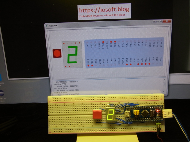
The target system in the demonstration is a ‘blue pill’ STM32F103 board, with a 7-segment display and pushbutton. This CPU board is particularly convenient because it has a 4-pin connector with SWD clock & data; it can be seen on the right-hand side of the photograph above.

The SWD connection is described in detail in this post, in brief, the circuit is:

ftdi_cable
SWD cable circuit diagram

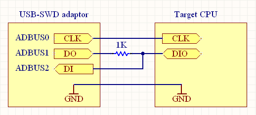
Take care when making any connections to power lines, especially the 5 volt line on the FTDI module; if mis-connected, high currents can flow, resulting in significant damage.

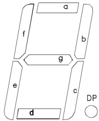
The demonstration system has a Kingbright SC56-11LGWA common-cathode 7-segment display; the anodes are driven directly from the CPU I/O pins with 220 ohm series resistors. The pin mapping (reading from top left of the display) is:

Segment   CPU Pin (via 220R)
g         PB11
f         PB10
a         PB1
b         PB0
e         PB12
d         PB13
c         PB14
DP        PB15

Button    PB3 (button shorts this pin to ground)

You may wonder why I have used such a complex mapping; why not use 8 consecutive pins? The answer is that the above arrangement makes the wiring easier, at the expense of a little software complexity. This trade-off is quite common in commercial projects, where the demands of cost-saving often lead to significant complexity in the hardware configuration.

Software

reporta

The full source code is available on Github, and is compatible with Python 2.7 or 3.x. It has been tested on Windows, and is theoretically Linux-compatible, except for a problem reading data back from USB, as described in the earlier blog – this issue needs to be resolved. The Python library dependencies are:

  • PyQt v4 or v5 (GPL version)
  • ftd2xx
  • pypiwin32 (if running Python 3.x)

These can be installed with ‘pip’ or ‘pip3’ as usual.

PyQt

The following text describes how I created the graphical front-end, for the benefit of anyone wishing to understand or modify the code; this isn’t necessarily the best way, it is just what I did based on past experience.

There are many options for creating a GUI in Python; I’ve used PyQt in the past, so that is the option I’ve chosen here. In case you’re unfamiliar with it, the current version is 5, but many installations are still version 4, so I’ve written the code to be compatible with both, even though this does involve some manipulation of the libraries:

try:
    from PyQt5.QtGui import QBrush, QPen, QColor, QFont, QTextCursor, QFontMetrics, QPainter
    from PyQt5.QtWidgets import QApplication, QGraphicsScene, QGraphicsView, QGraphicsSimpleTextItem
    from PyQt5 import QtCore, QtWidgets
except:
    from PyQt4.QtGui import QBrush, QPen, QColor, QFont, QTextCursor, QFontMetrics, QPainter
    from PyQt4.QtGui import QApplication, QGraphicsScene, QGraphicsView, QGraphicsSimpleTextItem
    from PyQt4 import QtCore, QtGui as QtWidgets

It is possible to create the entire front-end graphically using Qt designer, then just import the GUI file and it will be displayed exactly as designed, so in theory you only need to write the event-handlers for the various actions. Personally, I find this approach a bit tricky when implementing more complex GUIs, so tend to use the PyQt function calls to build the graphics from scratch.

Main Window

The main window is as simple as possible, containing only one central widget:

class MyWindow(QtWidgets.QMainWindow, MyWidget):
    graph_updater = QtCore.pyqtSignal(str)

    def __init__(self, parent=None):
        QtWidgets.QMainWindow.__init__(self, parent)
        self.widget = MyWidget(self)
        self.setCentralWidget(self.widget)
        self.setWindowTitle(VERSION)
        self.resize(*WINDOW_SIZE)
        self.graph_updater.connect(self.widget.update_graph)

A ‘graph_updater’ signal is defined so that any thread can send a request to update the graphics; this will be queued until the main GUI thread is back in control, so there is no ambiguity over which thread is performing the updates.

The single widget contains all the graphical elements, and the hierarchy is important if  they are to be displayed correctly; for example, if the window is resized, I want all the elements to be resized in proportion, and that is only possible if the correct parent-child relationship is maintained.

The upper area of the widget is graphics, the lower is text; they are combined using a vertical layout widget.

self.text = QtWidgets.QTextEdit()
self.scene = QGraphicsScene()
self.view = MyView(self.scene)
...
layout = QtWidgets.QVBoxLayout()
layout.addWidget(self.view, 30)
layout.addWidget(self.text, 10)
self.setLayout(layout)

Text display

The text area is used to display all kinds of diagnostic information, so it is convenient to redirect the console print function to display here. This is done by creating ‘write’ and ‘flush’ functions in the widget, which emit a signal linked to an updater function:

text_updater = QtCore.pyqtSignal(str)
...
self.text_updater.connect(self.update_text)
...
# Handler to update text display
def update_text(self, text):
    disp = self.text.textCursor()           # Move cursor to end
    disp.movePosition(QTextCursor.End)
    text = str(text).replace("\r", "")      # Eliminate CR
    while text:
        head,sep,text = text.partition("\n")# New line on LF
        disp.insertText(head)
        if sep:
            disp.insertBlock()
    self.text.ensureCursorVisible()    # Scroll if necessary

# Handle sys.stdout.write: update text display
def write(self, text):
    self.text_updater.emit(str(text))
def flush(self):
    pass

Now all that is necessary is to redirect console output to the main widget..

sys.stdout = self

..and magically anything in a ‘print’ function will appear in the text display. The PyQt Signal interface ensures there are no threading problems, you can still use the print function anywhere.

Graphical display

When displaying graphics, Qt (and hence PyQt) makes a distinction between the graphical objects (the ‘scene’) and their realisation on the screen (the ‘view’).

When first experimenting with background patterns, I discovered one (Dense1Pattern) that creates rows of holes similar to the prototyping board. Having fixed on this, it was logical to draw all objects with respect to this grid, i.e. in nominal units of 0.1 inches as on the prototyping board, though the graphics will expand or shrink when the window size is changed.

Drawing

To draw an object, it is just added to the scene, and it will automatically be displayed, for example to draw a circle:

# Add circle to grid, given centre
    def draw_circle(self, gpos, size, pen, brush=PIN_ON_BRUSH):
        size *= GRID_PITCH
        x,y = self.grid_pos(gpos)
        p = self.scene.addEllipse(0, 0, size, size, pen, brush)
        p.setPos(x-size/2.0, y-size/2.0)
        return p

You can see the conversions from screen-units to grid-units. One less-obvious aspect of this code is that the ellipse is originally drawn at the 0,0 origin, then moved into place, rather than being drawn at the final location; this simplifies any subsequent operations such as movement or rotation.

Animation

The drawing function returns the object that has been created, which must be saved somewhere, so it can be animated.  The most obvious form of animation is to replace that object with another, e.g. one drawn in dark red to light red, but there is an easier way to modify any drawn object: change the opacity – the extent to which the object is transparent or opaque. If a bright red object is drawn with an opacity value of 0.1, it becomes a faint dark red; changing the opacity to 1.0 restores the full strong colour.

So the objects that are to be animated are stored as a list in a dictionary, indexed on the signal name (e.g. ‘PB10’); when that signal changes state, it is only necessary to walk the list, setting the opacity as required.

# Set pin (or segment) on/off state
# Format is 'name=value', e.g.  'PA10=1'
def set_pin(self, s):
    name, eq, num = s.partition('=')
    if eq and name in self.sigpins:
        val = int(num, 16)
        for p in self.sigpins[name]:
            if int(p.opacity()) != val:
                p.setOpacity(PIN_ON_OPACITY if val else PIN_OFF_OPACITY)

7-segment display

As it happens, PyQt has a widget to draw 7-segment displays, but in this case it is easier to animate if drawn from scratch. The standard segment notation is:

sevenseg

To draw this in one continuous operation, I start with segment F, then ABCDEG. Once drawn, the list is rearranged into ABCDEFGH order, where H is the decimal point.

SWD interface

The SWD interface uses an FTDI USB device as described in detail here. The software used in this project is very similar, but has been optimised to scan the I/O ports quite fast, around 100 times per second. The way this has been achieved is to group all the commands to the FTDI device together, so a single block of data requests is sent out over the USB bus, then a single block of responses is read back.

All the outgoing requests are buffered, rather than being sent individually – this is quite a simple change, you just have to remember to flush the buffer before reading back the results. However you then have the problem that the returned data block consists of the data from several requests – how do you work out which data value corresponds to which request? The method I’ve adopted is to create a polling list, with objects representing the memory addresses to be polled

poll_vars = []  # List of variables to be polled

# Storage class for variable to be polled
class Pollvar(object):
    def __init__(self, name, addr):
        self.name, self.addr = name, addr
        self.value = None

# Add variable to the polling list
def poll_add_var(name, addr):
    poll_vars.append(Pollvar(name, addr))

The data requests are generated by walking down the list, then when the responses arrive, the ‘value’ fields are filled in sequentially, or set to ‘none’ if there was an error.

# Send out poll requests
def poll_send_requests(h):
    for pv in poll_vars:
        swd.swd_wr(h, swd.SWD_AP, APORT_TAR, pv.addr, True, False)
        swd.swd_idle_bytes(h, 2)
        swd.swd_rd(h, swd.SWD_AP, APORT_DRW, True, False)
        swd.swd_rd(h, swd.SWD_AP, APORT_DRW, True, False)

# Get poll responses
def poll_get_responses(h):
    for pv in poll_vars:
        swd.swd_wr(h, swd.SWD_AP, APORT_TAR, pv.addr, False, True)
        swd.swd_rd(h, swd.SWD_AP, APORT_DRW, False, True)
        req = swd.swd_rd(h, swd.SWD_AP, APORT_DRW, False, True)
        pv.value = req.data.value if (req.data is not None and
                    req.ack.value==swd.SWD_ACK_OK) else None

It is slightly confusing that the request & response use the same swd_wr and swd_rd functions; the key to understanding this code is to look at the boolean values. ‘True, False’ means that a transmission is sent, but no data is read back; ‘False, True’ is the opposite, in that nothing is sent, the response is just read back.

If you want to see the SWD transactions, try setting swd.VERBOSE to True:

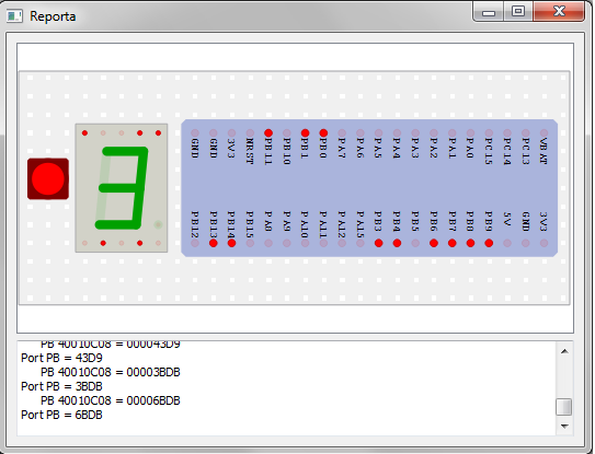
SWD interface: FT232H device in Single RS232-HS
Reporta

Rd 0 IDCODE  1BA01477 Ack 1
Wr 0 ABORT   0000001E Ack 1
Wr 4 CTRL    50000000 Ack 1
Rd 4 STATUS  F0000040 Ack 1
DP ident: 1BA01477
Wr 8 SELECT  000000F0 Ack 1
Rd C DRW/BD3 00003BDB Ack 1
Rd C DRW/BD3 14770011 Ack 1
AP ident: 14770011
Wr 8 SELECT  00000000 Ack 1
Wr 0 CSW/BD0 22000002 Ack 1
Wr 4 TAR/BD1 40010C08
Rd C DRW/BD3
Rd C DRW/BD3
Wr 4 TAR/BD1 40010C08 Ack 1
Rd C DRW/BD3 14770011 Ack 1
Rd C DRW/BD3 000043D9 Ack 1
..and so on..

Looking at the last block of 6 transactions, the first 3 are a write-cycle to the SWD TAR (transfer address) register, then a dummy read and the actaul read cycle. These are the requests being sent to the target system; nothing is being read back so the read-data & ack-status values are unknown. The second block of 3 are the readback of these requests, so the actual values are displayed.

An ‘ack’ value of anything apart from 1 is an error; a value of 0 or 7 suggests the target isn’t responding, 2 means it is trying to send a delayed response, and 4 indicates a hard error – this is sticky, so will persist until cleared by writing to the ‘abort’ register.

Code structure

The ‘reporta’ project source files on Github are:

reporta.py:   main program
rp_pyqt.py:   PyQt interface
rp_arm.py:    ARM processor definitions
rp_swd.py:    SWD interface
rp_ftd2xx.py: FTDI device driver

The lower 3 files are very similar to their counterparts in these posts, basically I’ve copied the files with minor modifications. Each file has a ‘main’ function to demonstrate its functionality; for example, you can see the PyQt interface running without the FTDI hardware, just by executing rp_pyqt.py

The main ‘reporta’ program has no command-line options, currently the I/O port of interest is hard-coded; to add other ports (or CPU memory locations) to the polling list, just use the poll_add_var function.

As with the previous posts, I must state that so far I’ve only tested this technique on the STM32F103 processors; others may require custom powerup sequences, or special incantations to gain access to the CPU memory – but hopefully my Python code will provide a useful starting-point.

Copyright (c) Jeremy P Bentham 2018. Please credit this blog if you are using the information or software in it.

Programming FTDI devices in Python: Part 5

Doing something useful with SWD

In part 4 we got as far as reading in the CPU identification, which is of no real use; in this part we’ll actually read some of the CPU internals, but first we need to understand how SWD accesses are controlled.

Exif_JPEG_PICTURE
SWD cable showing resistor

DAP: DP and AP

You may think that we just need to feed a 32-bit address into the SWD port, and get a value back, but the reality is much more complicated. The SWD clock & data lines are connected to the CPU Debug Port (SW-DP), which has its own address space. Read/write accesses to the CPU memory aren’t controlled by the DP; you have to go through the Access Port (AP), which also has a separate memory space, and is bank-switched.

DP

We’ve already accessed the Debug Port ID code register, the other read-write registers are:

# Debug Port (SWD-DP) registers
# See ARM DDI 0314H "Coresight Components Technical Reference Manual"
DPORT_IDCODE        = 0x0   # ID Code / abort
DPORT_ABORT         = 0x0
DPORT_CTRL          = 0x4   # Control / status
DPORT_STATUS        = 0x4
DPORT_SELECT        = 0x8   # Select
DPORT_RDBUFF        = 0xc   # Read buffer

These registers control various aspects of the debug interface, for example the ‘abort’ register is used to reset the internal logic after an error, and the ‘control’ register is used to power up the peripherals needed for debugging.

The ‘select’ register has bitfields to control AP and DP bank-switching; it is convenient to define this using CTYPES:

from ctypes import Structure, Union, c_uint
# AHB-AP Select Register
class DP_SELECT_REG(Structure):
    _fields_ = [("DPBANKSEL",   c_uint, 4),
                ("APBANKSEL",   c_uint, 4),
                ("Reserved",    c_uint, 16),
                ("APSEL",       c_uint, 8)]
class DP_SELECT(Union):
    _fields_ = [("reg",   DP_SELECT_REG),
                ("value", c_uint)]
dp_select = DP_SELECT()

The union allows us to specify the whole 32–bit register when doing SPI read & write cycles, but still access individual bitfields within it.

AP

The AP registers are:

# Access Port (AHB-AP) registers, high nybble is bank number
# See ARM DDI 0337E: Cortex M3 Technical Reference Manual page 11-38
APORT_CSW           = 0x0   # Control status word
APORT_TAR           = 0x4   # Transfer address
APORT_DRW           = 0xc   # Data read/write
APORT_BANK0         = 0x10  # Banked registers
APORT_BANK1         = 0x14
APORT_BANK2         = 0x18
APORT_BANK3         = 0x1c
APORT_DEBUG_ROM_ADDR= 0xf8   # Address of debug ROM
APORT_IDENT         = 0xfc   # AP identification

The Control Status Word register controls various aspects of the CPU memory accesses, for example the data size, and auto-increment for reading blocks of memory:

# AHB-AP Control Status Word Register
class AP_CSW_REG(Structure):
    _fields_ = [("Size", c_uint, 3),
                ("Res1", c_uint, 1),
                ("AddrInc", c_uint, 2),
                ("DbgStatus", c_uint, 1),
                ("TransInProg", c_uint, 1),
                ("MODE", c_uint, 4),
                ("Res2", c_uint, 13),
                ("HProt1", c_uint, 1),
                ("Res3", c_uint, 3),
                ("MasterType", c_uint, 1),
                ("Res4", c_uint, 2)]
class AP_CSW(Union):
    _fields_ = [("reg", AP_CSW_REG),
                ("value", c_uint)]
ap_csw = AP_CSW()

Because the AP can be accessing main CPU memory, it has two time-dependencies:

  • the AP may return a ‘wait’ indication in the status field so the transaction has time to go though
  • the data isn’t returned immediately; first you have to do a dummy read cycle, then a second read cycle that actually returns the data

So to set up a CPU memory read cycle, we need to configure the AP (including its bank-switching) then set a transfer address

# Configure AP memory accesses
def ap_config(d, inc, size):
    dp_select.reg.APBANKSEL = 0     # Zero bank
    swd.swd_wr(d, swd.SWD_DP, DPORT_SELECT, dp_select.value)
    ap_csw.reg.MasterType = 1
    ap_csw.reg.HProt1 = 1           # Enable incrementing, set access size
    ap_csw.reg.AddrInc = 1 if inc else 0
    ap_csw.reg.Size = 0 if size==8 else 1 if size==16 else 2
    return swd.swd_wr(d, swd.SWD_AP, APORT_CSW, ap_csw.value)

# Set AP memory address
def ap_addr(d, addr):
    swd.swd_wr(d, swd.SWD_AP, APORT_TAR, addr)
    swd.swd_idle_bytes(d, 2)            # Idle to avoid 'wait' response

# Do an immediate read of a 32-bit CPU memory location
def cpu_mem_read32(d, addr):
    ap_addr(d, addr)                              # Address to read
    swd.swd_rd(d, swd.SWD_AP, APORT_DRW)          # Dummy read cycle
    r = swd.swd_rd(d, swd.SWD_AP, APORT_DRW)      # Read data
    return r.data.value if r.ack.value==swd.SWD_ACK_OK else None

There are 2 idle (null) bytes after the target memory address is set. These give the AP time to process the address value before it is used; if omitted, the AP gives an ack value of 2 (‘wait’) on the next transaction.

User interface

The console-based user interface is minimal; it just allows you to specify the STM32F103  GPIO port or memory address to be accessed, e.g.

python ftdi_py_part5.py gpiob
DP ident: ack 1, value 1BA01477h
Powerup:  ack 1, value F0000040h
AP ident: ack 1, value 14770011h
40010C00: GPIOB CRL=44488433 CRH=33333344 IDR=00007FDA ODR=00007C1A

python ftdi_py_part5.py 0
DP ident: ack 1, value 1BA01477h
Powerup:  ack 1, value F0000040h
AP ident: ack 1, value 14770011h
00000000: 20005000

If a gpio port is specified, four of its register values are printed out (CRL, CRH, IDR, ODR); the other diagnostic values can be useful if the access fails. Further help is available by setting the VERBOSE flag at the top of the part 4 file, which enables a printout of all the SWD cycles:

# Command line with invalid address
python ftdi_py_part5.py 800000 
  Rd 0 IDCODE  1BA01477 Ack 1
DP ident: ack 1, value 1BA01477h
  Wr 0 ABORT   0000001E Ack 1
  Wr 4 CTRL    50000000 Ack 1
  Rd 4 STATUS  F0000000 Ack 1
Powerup:  ack 1, value F0000000h
  Wr 8 SELECT  000000F0 Ack 1
  Rd C DRW/BD3 00000000 Ack 1
  Rd C DRW/BD3 14770011 Ack 1
AP ident: ack 1, value 14770011h
  Wr 8 SELECT  00000000 Ack 1
  Wr 0 CSW/BD0 22000012 Ack 1
  Wr 4 TAR/BD1 00800000 Ack 1
  Rd C DRW/BD3 14770011 Ack 1
  Rd C DRW/BD3 00000000 Ack 4
00800000: ?

Source code

Here is the final batch of source-code. I’ve only tested the it with STM32F1 CPUs, so if you are trying to communicate with something else, there is a strong possibility you’ll need to make some changes. Points to bear in mind:

  1. Check the the CPU supports SWD, and the connections it uses.
  2. Check for any special power-up requirements, e.g. sending the reset sequence multiple times, or setting registers to enable debugging mode
  3. Check that the SWD clock and signal lines are toggling OK.
  4. Watch out for acknowledgement values 2 and 4, indicating a problem.
  5. Once an error occurs, it will persist over successive cycles until reset by writing to the ABORT register.
  6. Good luck!
# Python FTDI SWD CPU memory read from iosoft.blog
# Compatible with Python 2.7 or 3.x
#
# v0.01 JPB 8/12/18

import sys, ftdi_py_part3 as ft, ftdi_py_part4 as swd
from ctypes import Structure, Union, c_uint

# STM32F1 address values for testing
# Address of GPIO Ports A - E on STM32F1
ports = {"GPIOA":0x40010800, "GPIOB":0x40010C00, "GPIOC":0x40011000,
         "GPIOD":0x40011400, "GPIOE":0x40011800}
# GPIO registers at offsets 0, 4, 8, 12
gpio_regs = ("CRL", "CRH", "IDR", "ODR")

# Debug Port (SWD-DP) registers
# See ARM DDI 0314H "Coresight Components Technical Reference Manual"
DPORT_IDCODE        = 0x0   # ID Code / abort
DPORT_ABORT         = 0x0
DPORT_CTRL          = 0x4   # Control / status
DPORT_STATUS        = 0x4
DPORT_SELECT        = 0x8   # Select
DPORT_RDBUFF        = 0xc   # Read buffer

# Access Port (AHB-AP) registers, high nybble is bank number
# See ARM DDI 0337E: Cortex M3 Technical Reference Manual page 11-38
APORT_CSW           = 0x0   # Control status word
APORT_TAR           = 0x4   # Transfer address
APORT_DRW           = 0xc   # Data read/write
APORT_BANK0         = 0x10  # Banked registers
APORT_BANK1         = 0x14
APORT_BANK2         = 0x18
APORT_BANK3         = 0x1c
APORT_DEBUG_ROM_ADDR= 0xf8   # Address of debug ROM
APORT_IDENT         = 0xfc   # AP identification

# DP Select Register
class DP_SELECT_REG(Structure):
    _fields_ = [("DPBANKSEL",   c_uint, 4),
                ("APBANKSEL",   c_uint, 4),
                ("Reserved",    c_uint, 16),
                ("APSEL",       c_uint, 8)]
class DP_SELECT(Union):
    _fields_ = [("reg",   DP_SELECT_REG),
                ("value", c_uint)]
dp_select = DP_SELECT()

# AHB-AP Control Status Word Register
class AP_CSW_REG(Structure):
    _fields_ = [("Size",        c_uint, 3),
                ("Res1",        c_uint, 1),
                ("AddrInc",     c_uint, 2),
                ("DbgStatus",   c_uint, 1),
                ("TransInProg", c_uint, 1),
                ("MODE",        c_uint, 4),
                ("Res2",        c_uint, 13),
                ("HProt1",      c_uint, 1),
                ("Res3",        c_uint, 3),
                ("MasterType",  c_uint, 1),
                ("Res4",        c_uint, 2)]
class AP_CSW(Union):
    _fields_ = [("reg",   AP_CSW_REG),
                ("value", c_uint)]
ap_csw = AP_CSW()

# Select AP bank, do read cycle
def ap_banked_read(d, addr):
    dp_select.reg.APBANKSEL = addr >> 4;
    swd.swd_wr(d, swd.SWD_DP, DPORT_SELECT, dp_select.value)
    swd.swd_rd(d, swd.SWD_AP, addr&0xf)
    return swd.swd_rd(d, swd.SWD_AP, addr&0xf)

# Configure AP memory accesses
def ap_config(d, inc, size):
    dp_select.reg.APBANKSEL = 0     # Zero bank
    swd.swd_wr(d, swd.SWD_DP, DPORT_SELECT, dp_select.value)
    ap_csw.reg.MasterType = 1
    ap_csw.reg.HProt1 = 1           # Enable incrementing, set access size
    ap_csw.reg.AddrInc = 1 if inc else 0
    ap_csw.reg.Size = 0 if size==8 else 1 if size==16 else 2
    return swd.swd_wr(d, swd.SWD_AP, APORT_CSW, ap_csw.value)

# Set AP memory address
def ap_addr(d, addr):
    swd.swd_wr(d, swd.SWD_AP, APORT_TAR, addr)
    swd.swd_idle_bytes(d, 2)            # Idle to avoid 'wait' response

# Do an immediate read of a 32-bit CPU memory location
def cpu_mem_read32(d, addr):
    ap_addr(d, addr)                              # Address to read
    swd.swd_rd(d, swd.SWD_AP, APORT_DRW)          # Dummy read cycle
    r = swd.swd_rd(d, swd.SWD_AP, APORT_DRW)      # Read data
    return r.data.value if r.ack.value==swd.SWD_ACK_OK else None

if __name__ == "__main__":
    mem = sys.argv[1].upper() if len(sys.argv) > 1 else None
    dev = ft.ft_open()
    if not dev:
        print("Can't open FTDI device")
        sys.exit(1)
    ft.set_bitmode(dev, 0, 2)           # Enable SPI
    ft.set_spi_clock(dev, 1000000)      # Set SPI clock
    ft.ft_write(dev, (0x80, 0, ft.OPS)) # Set outputs
    swd.swd_reset(dev)                  # Send SWD reset sequence
    resp = swd.swd_rd(dev, swd.SWD_DP, DPORT_IDCODE) # Request & response
    if resp is None:
        print("No response")
    else:
        print("DP ident: ack %u, value %08Xh" % (resp.ack.value, resp.data.value))
        swd.swd_wr(dev, swd.SWD_DP, DPORT_ABORT, 0x1e)    # Clear errors
        swd.swd_wr(dev, swd.SWD_DP, DPORT_CTRL,  0x5<<28) # Powerup request
        resp = swd.swd_rd(dev, swd.SWD_DP, DPORT_STATUS)  # Get status
        print("Powerup:  ack %u, value %08Xh" % (resp.ack.value, resp.data.value))
        resp = ap_banked_read(dev, APORT_IDENT)           # Get AP ident
        print("AP ident: ack %u, value %08Xh" % (resp.ack.value, resp.data.value))
        ap_config(dev, 1, 32);                            # Configure AP RAM accesses
        s = ""
        if mem in ports:
            addr = ports[mem]
            s = "%08X: %s" % (addr, mem)
            for reg in gpio_regs:
                val = cpu_mem_read32(dev, addr)
                s += " %s=%08X" % (reg, val)
                addr += 4
        else:
            try:
                addr = int(mem, 16)
            except:
                addr = None
            if addr is not None:
                s = "%08X:" % addr
                val = cpu_mem_read32(dev, addr)
                s += " %08X" % val if val is not None else " ?"
        print(s)   

    dev.close()

# EOF

Next steps

Whilst this code is an interesting framework for experimentation, it lacks some of the features and error-handling of a ‘real’ application, for example it’d be nice to draw an animated picture of the CPU, showing the SWD poll results graphically. That is the subject of another post.

Copyright (c) Jeremy P Bentham 2018. Please credit this blog if you are using the information or software in it.

Programming FTDI devices in Python: Part 4

First steps toward viewing CPU internals with SWD

What is SWD?

If you want to access the internals of a programmable device, there used to be only one way: a JTAG interface. This uses 4 signals: TDI, TDO, TCK and TMS, and is quite complex; it can handle multiple daisy-chained devices, of various types. When you add in a variety of USB-JTAG adaptors and APIs to serve data to higher-level GUIs, you have a very complex piece of software; for an illustration of this, take a look at OpenOCD

More recently, ARM introduced a simpler 2-wire protocol, called SWD. It has just 2 connections, clock and bi-directional data, but has most of the capabilities of the older JTAG systems. Software such as OpenOCD has been extended to incorporate the SWD protocol, but is still very complex; I felt there was a need for a simple-as-possible implementation, in a high-level language, that could easily be combined with custom GUI to display the CPU internals in whatever fashion suits your application; maybe an animated diagram of the CPU, display of serial data streams, or graphs of analogue values.

So the Python SWD project was born, and I needed to select a USB device for the interface. The more modern FTDI parts have the MPSSE protocol engine, which (as we’ll see later) is ideally suited for the SWD protocol, and there are a wide variety of FTDI cables and modules at reasonable cost.

In the previous blog posts I’ve documented some preliminary steps to understand the FTDI hardware, and how it can be driven from Python; now we have a major test, implementing the SWD protocol.

Hardware

Exif_JPEG_PICTURE
FTDI adaptors

We’ll only be using 3 pins (clock, data out, data in) on the adaptor, so it isn’t difficult to wire up and FTDI cable or module, the only requirements are that the device supports the MPSSE protocol, and has a 3.3V output. If the module has a 5 volt pin, you do need to be careful not to short-circuit or mis-connect it, as it can source quite high currents (over an amp) and do significant damage. If you peer closely at the above diagram, you’ll see top-right an Adafruit FT232H module with connector pins fitted but missing pin 1; this is so I can’t accidentally destroy my test CPU by accidentally connecting the SWD to 5 volts.

In the introduction I mentioned that the SWD protocol has a bi-directional data line, but unfortunately the FTDI adaptors don’t provide a bi-directional mode – we need to combine the data input & output lines to provide this. This is done by putting a resistor in series with the FTDI output, so that the target system can pull that line high or low when required.

ftdi_cable
SWD cable circuit diagram
Exif_JPEG_PICTURE
SWD cable with heatshrink pulled back to show DI-DO resistor

A similar scheme is mentioned in the OpenOCD documentation, but they suggest a value of 470 ohms. I’ve gone with 1K because at its lowest drive setting, FTDI chips such as the FT232H only source 4 mA, and I’m never keen on overloading outputs, no matter how harmless this is supposed to be – but feel free to follow the majority opinion, and go with 470 ohms.

Some people suggest that is is necessary for the FTDI adaptor and target CPU to share a common supply. Professional JTAG adaptors do this – they take a supply from the target system, and use level-shifters to ensure the signals are of the right amplitude – but it should’t be necessary providing your supplies are of reasonable quality. However, you must resist the temptation to make the cables very long; we’re dealing with fast edge-sensitive signals, so I’d keep the cable length below 6 inches (150 mm).

A convenient way of incorporating the resistor in a cable is by soldering & covering with heat-shrink tubing; at a pinch you could use a screw-terminal block, but try to keep the assembly reasonably compact to avoid EMC problems.

SWD Protocol

There are 3 main difficulties with this protocol:

  • Bit-oriented rather than byte-oriented
  • Bi-directional data line
  • Intolerant of errors

The first of these is quite a culture-shock; when dealing with bit values, they are usually aggregated up to the nearest byte or word. This isn’t good enough for SWD; if you are supposed to be sending 2 bits, it must be 2 bits, not padded out to the nearest byte.

The second issue makes debugging the software quite challenging; if there is a bug that causes both sides to transmit at the same time, it is difficult to work out which side is at fault.

The third issue is actually a design feature; in the event of an error, the CPU interface is designed to stop transmitting, to avoid further data collisions – but when writing your own code, you often find the target CPU stops talking; it refuses to communicate, and you don’t know why.

To give an example, here is the standard SWD read transaction on which all data transfers are based, taken from the original ARM document “Serial Wire Debug and the CoreSight Debug and Trace Architecture”. All transactions are initiated and controlled by the SWD adaptor, the target CPU just ‘fills in the blanks’ in the messages it is given.

swd_read

We start with the data line being idle, which (very confusingly) can be either high or low. The clock line can be either be running continuously, or can stop between transactions; a bit like Ethernet, in that the recipient looks for a specific marker in the data, and ignores everything until that is received. In this context, the marker is at least 2 low (zero) bits, followed by a high ‘start’ bit, then there are 7 bits of header data. If you want to know the meaning of these bits, ARM have copious online documentation, such as the “CoreSight Components Technical Reference Manual”.

After the initial transmission to the CPU, the adaptor inserts a dummy ‘turnaround’ bit where it stops driving the data line, letting the target CPU take over. The adaptor continues toggling the clock line while the CPU sends 3 acknowledgement bits; if these show a positive response (100, l.s.bit first, so a value of 1) then 32 bits of data will follow, and a parity bit. This concludes the transaction, but another turnaround bit is needed so the SWD adaptor can start driving the bus again.

Alternatively, the acknowledgement bits may show an error (001, which is a value of 4), in which case the CPU will stop communicating, or a ‘wait’ indication (010, a value of 2), which means the data isn’t yet available – try again later.

After this transaction, another may follow immediately, or a minimum of 2 zero bits may be inserted to idle the data line – a clean transition between transactions is essential, with no spurious additional bits.

Python implementation

After several false starts, I ended up creating my own class to store bit values; there are various bit-handling libraries around, but my requirements are so simple that these are massive overkill.

# Class for a multi-bit value
class Bitval(object):
    def __init__(self, value, nbits, name="", rd=False):
        self.value = value
        self.nbits = nbits
        self.name = name
        self.rd = rd

That’s all – it is just a vehicle for storing one or more bits; the ‘name’ isn’t strictly necessary, but is useful in identifying one bit-value amongst many others.

The ‘rd’ flag indicates whether the value should be write-only, or whether we need the value to be read back from the target system. For example, in the SWD read cycle above, we need to know the ‘ack’ and ‘data’ values, but aren’t really interested in reading back the other bits we’re sending – and the FTDI device provides a convenient way of controlling whether input data is read back or not (command bit 5: ‘TDO/DI data input’).

Creating the SWD request is just a question of stacking the bit-values in a list, e.g.

# 1 start bit, 1 AP bit, 1 read bit, 2 address bits...
Bitval(1, 1, "Start"),      Bitval(ap,   1, "AP"),
Bitval(1, 1, "Read"),       Bitval(addr, 2, "Addr"), etc..

Our USB driver software just churns out the bit-values in sequence, then gets any responses that are required; it doesn’t need to understand what each bit-value means. All that is needed is a bit of support code, to allow iteration through the list, and give access to the important element values:

# Create an SWD read request for a given AP or DP address
class swd_rd_request(object):
    def __init__(self, ap, addr):
        addr >>= 2
        hpar = ap ^ 1 ^ (addr & 1) ^ (addr>>1 & 1)
        self.ack = Bitval(0, 3, "Ack", 1)
        self.data = Bitval(0, 32, "Data", 1)
        self.dparity = Bitval(0, 1, "DParity", 1)
        self.bitvals = (
            Bitval(1, 1, "Start"),      Bitval(ap, 1, "AP"),
            Bitval(1, 1, "Read"),       Bitval(addr, 2, "Addr"),
            Bitval(hpar, 1, "HParity"), Bitval(0, 1, "Stop"),
            Bitval(1, 1, "Park"),       Bitval(0, 1, "Turn"),
            self.ack,                   self.data,
            self.dparity,               Bitval(0, 1, "Turn"))

    # Allow the bitval list to be iterated
    def __getitem__(self, idx):
        bv = self.bitvals[idx]
        return bv

Having set up a class for our data transaction, it is easy to transmit the data, and evaluate the response:

req = swd_rd_request(ap, addr)  # Create request
for bv in req:                  # For each bit-value..
    spi_write_bitval(h, bv)     # ..send bit(s) out
for bv in req:                  # For each bit-value..
    if bv.rd:                   # .. with 'rd' flag set..
        spi_read_bitval(h, bv)  # .. read bit(s) in

Since the request is a class instance, we can access the returned bits in an intuitive way, e.g. simplistically:

if req.ack.value == 1:     # If request was acknowledged OK..
    print(req.data.value)  # ..print returned data value

SWD reset

Now that we have an easy way to send an SWD request, can we read something out from the CPU? Nearly, there is just the reset process to go through.

To unlock the CPU SWD interface and start communicating, we need to send a lengthy bit sequence, namely at least 50 ‘1’ bits, then 0111 1001 1110 0111 (9E E7 hex, l.s.bit first), then at least another 50 ‘1’ bits, then at least 2 ‘0’ bits. this serves 2 purposes:

  • It provides a unique bit-pattern, that can’t be confused with a normal request
  • It gives time for the CPU SWD interface to be powered up

The second point is important; ARM CPUs are designed with power-saving in mind, and parts of the CPU may be powered down when not in use, so need some time to wake up. This especially applies if the CPU is in a deep sleep mode; it may require the startup sequence to be sent several times before the CPU is sufficiently awake to respond to requests. Despite the ‘reset’ name, this sequence does not reset the error-handling of the SWD interface; that must be done using a separate write-cycle.

Reading the CPU ID

After sending the startup sequence, the first request should be a read of the CPU ID; not just because it is a simple read-only value, but also because the CPU specification may require that it be read before anything else.

We need to set the ‘ap’ and ‘addr’ values in the code above; I’ll describe these settings in detail in the next post, but for now, it is sufficient to say that the ID register is at DP address 0, so ap=0, addr = 0.

So we just need to send the startup bit pattern, then a request with these values, and read back the result. If we’re unlucky, it’ll be all-0s because the target CPU isn’t communicating, or all-1s because the data line is floating; ideally it is something between those, that is consistent every time it is read; on an STMicro Cortex M3 CPU (STM32F103) it is 1BA01477, see your CPU’s data sheet for the corresponding value.

See below for the full Python source code to read the ID register; I can’t claim this code is particularly useful on its own, but in the next post we’ll start to explore some more useful data requests.

Regrettably the code doesn’t work on Linux with libftdi. In all my tests the SPI write cycles work fine, but the read cycles always return null data. To be investigated.

# Python FTDI SWD example from iosoft.blog
# Compatible with Python 2.7 or 3.x
#
# v0.01 JPB 8/12/18

import time, ftdi_py_part3 as ft

VERBOSE  = False    # Flag to display SWD read/write cycles
ERRVAL = 0xEEEEEEEE # Dummy value returned if read cycle fails

SWD_DP          = 0     # AP/DP flag bits
SWD_AP          = 1
DPORT_IDCODE    = 0x0   # ID Code address

SWD_ACK_OK      = 1     # SWD Ack values
SWD_ACK_WAIT    = 2
SWD_ACK_ERROR   = 4

FTDI_MODE_BITBANG   = 1     # MPSSE modes
FTDI_MODE_MPSSE     = 2

FTDI_SPI_WR_CLK_NEG = 0x01  # SPI command bit values
FTDI_SPI_BIT_MODE   = 0x02
FTDI_SPI_RD_CLK_NEG = 0x04
FTDI_SPI_LSB_FIRST  = 0x08
FTDI_SPI_WR_TDI     = 0x10
FTDI_SPI_RD_TDO     = 0x20
FTDI_SPI_WR_TMS     = 0x40

# Commands to read, write, and read+write SPI data
SPI_WR_BYTES    = FTDI_SPI_WR_CLK_NEG|FTDI_SPI_LSB_FIRST|FTDI_SPI_WR_TDI
SPI_RD_BYTES    = FTDI_SPI_LSB_FIRST|FTDI_SPI_RD_TDO
SPI_RD_WR_BYTES = SPI_RD_BYTES|SPI_WR_BYTES
SPI_RD_BITS     = SPI_RD_BYTES|FTDI_SPI_BIT_MODE
SPI_WR_BITS     = SPI_WR_BYTES|FTDI_SPI_BIT_MODE
SPI_RD_WR_BITS  = SPI_RD_BITS|SPI_WR_BITS

# Class for a bit value (1 - 32 bits)
class Bitval(object):
    def __init__(self, value, nbits, name="", rd=False):
        self.value = value
        self.nbits = nbits
        self.name = name
        self.rd = rd

# Send SWD reset; at least 50 high bits around 0111 1001 1110 0111
# (9E E7 lsb-first), then at least 2 null bits before start bit
def swd_reset(d):
    rst = (0xFF,0xFF,0xFF,0xFF,0xFF,0xFF,0xFF, 0x9E,0xE7,
           0xFF,0xFF,0xFF,0xFF,0xFF,0xFF,0xFF)
    spi_write_bytes(d, SPI_WR_BYTES, rst)
    spi_write_bits(d, SPI_WR_BITS, 0, 4)

# Send a number of idle (zero) bytes
def swd_idle_bytes(d, n):
    data = n * [0]
    spi_write_bytes(d, SPI_WR_BYTES, data)

# Create an SWD read request for a given AP or DP address
class swd_rd_request(object):
    def __init__(self, ap, addr):
        addr >>= 2
        hpar = ap ^ 1 ^ (addr & 1) ^ (addr>>1 & 1)
        self.ack = Bitval(0, 3, "Ack", 1)
        self.data = Bitval(0, 32, "Data", 1)
        self.dparity = Bitval(0, 1, "DParity", 1)
        self.bitvals = (
            Bitval(1,    1, "Start"),  Bitval(ap,   1, "AP"),
            Bitval(1, 1, "Read"),      Bitval(addr, 2, "Addr"),
            Bitval(hpar, 1, "HParity"),Bitval(0, 1, "Stop"),
            Bitval(1,    1, "Park"),   Bitval(0,    1, "Turn"),
            self.ack,                  self.data,
            self.dparity,              Bitval(0, 1, "Turn"))

    # Allow the bitval list to be iterated
    def __getitem__(self, idx):
        bv = self.bitvals[idx]
        return bv

# Create an SWD write request for a given AP or DP address
class swd_wr_request(object):
    def __init__(self, ap, addr, value):
        addr >>= 2
        hpar = ap ^ (addr & 1) ^ (addr>>1 & 1)
        self.ack = Bitval(0, 3, "Ack", 1)
        self.data = Bitval(value, 32, "Data")
        self.dparity = Bitval(parity32(value), 1, "DParity")
        self.bitvals = (
            Bitval(1,    1, "Start"),  Bitval(ap,   1, "AP"),
            Bitval(0, 1, "Read"),      Bitval(addr, 2, "Addr"),
            Bitval(hpar, 1, "HParity"),Bitval(0, 1, "Stop"),
            Bitval(1,    1, "Park"),   Bitval(0,    1, "Turn"),
            self.ack,                  Bitval(0,    1, "Turn"),
            self.data,                 self.dparity)

    # Allow the bitval list to be iterated
    def __getitem__(self, idx):
        bv = self.bitvals[idx]
        return bv

# Send an SWD read request and/or get the response
def swd_rd(d, ap, addr, tx=True, rx=True):
    req = swd_rd_request(ap, addr)
    ok = False
    if tx:
        spi_write_bitvals(d, req)
        ok = True
    if rx:
        ok = spi_read_bitvals(d, req)
    if VERBOSE:
        if rx:
            print("  Rd %X %-7s %08lX Ack %u" % (addr,
                  apreg_str(addr) if ap else dpreg_str(addr, 1),
                  req.data.value, req.ack.value))
        else:
            print("  Rd %X %-7s" % (addr,
                  apreg_str(addr) if ap else dpreg_str(addr, 1)))
    return req if ok else None

# Send an SWD write request and/or get the response
def swd_wr(d, ap, addr, value, tx=True, rx=True):
    req = swd_wr_request(ap, addr, value)
    ok = False
    if tx:
        spi_write_bitvals(d, req)
        ok = True
    if rx:
        ok = spi_read_bitvals(d, req)
    if VERBOSE:
        if rx:
            print("  Wr %X %-7s %08lX Ack %u" % (addr,
                  apreg_str(addr) if ap else dpreg_str(addr, 0),
                  req.data.value, req.ack.value))
        else:
            print("  Wr %X %-7s %08lX" % (addr,
                  apreg_str(addr) if ap else dpreg_str(addr, 0),
                  req.data.value))
    return req if ok else None

# Return DP register string
def dpreg_str(reg, rd):
    if rd:
        s = ("IDCODE" if reg==0 else "STATUS" if reg==4 else
             "RESEND" if reg==8 else "RDBUFF")
    else:
        s = ("ABORT " if reg==0 else "CTRL" if reg==4 else
             "SELECT" if reg==8 else "RDBUFF")
    return s

# Return AP register string; see Cortex-M3 'AHB-AP programmers model'
def apreg_str(reg):
    return ("CSW/BD0" if reg==0 else "TAR/BD1" if reg==4 else
            "BD2/RAR" if reg==8 else "DRW/BD3")

# Write bitval requests
def spi_write_bitvals(d, bitvals):
    for bv in bitvals:
        spi_write_bitval(d, bv)

# Read bitval responses
def spi_read_bitvals(d, bitvals):
    ok = True
    for bv in bitvals:
        ok = spi_read_bitval(d, bv)
        if not ok:
            break
    return ok

# Write a bit value to SPI interface
# If read-flag is set, use read+write, otherwise just write
def spi_write_bitval(d, bv):
    value, nbits = bv.value, bv.nbits
    cmd = SPI_RD_WR_BITS if bv.rd else SPI_WR_BITS
    while nbits > 0:
        n = min(nbits, 8)
        spi_write_bits(d, cmd, value&0xff, n)
        value >>= n
        nbits -= n

# Read a bit value (max 32 bits) from SPI, if read-flag is set
def spi_read_bitval(d, bv):
    ok = True
    if bv.rd:
        bv.value = shift = 0
        nbits = bv.nbits
        while ok and nbits >= 8:    # Get whole bytes
            data = spi_read_bytes(d, 1)
            if len(data) > 0:
                byt = data[0] >> max(8-nbits, 0)
                bv.value |= byt  0:
                bv.value = data[0]
            else:
                bv.value = ERRVAL
                ok = False
    return ok

# Write SPI command and data bytes to the device
def spi_write_bytes(d, cmd, data):
    n = len(data) - 1
    ft.ft_write(d, [cmd, n&0xff, n>>8] + list(data))

# Read data bytes back from SPI
def spi_read_bytes(d, nbytes):
    return ft.ft_read(d, nbytes)

# Write SPI command and up to 8 bits to the device
def spi_write_bits(d, cmd, byt, nbits):
    ft.ft_write(d, (cmd, nbits-1, byt))

# Read data bits back from SPI
# Bits are left-justified in the byte, so must be shifted down
def spi_read_bits(d, nbits):
    data = ft.ft_read(d, 1)
    return [data[0] >> (8-nbits)] if len(data)>0 else []

# Calculate parity of 32-bit integer
def parity32(i):
    i = i - ((i >> 1) & 0x55555555)
    i = (i & 0x33333333) + ((i >> 2) & 0x33333333)
    i = (((i + (i >> 4)) & 0x0F0F0F0F) * 0x01010101) >> 24
    return i & 1

if __name__ == "__main__":
    dev = ft.ft_open()
    if not dev:
        print("Can't open FTDI device")
    else:
        ft.set_bitmode(dev, 0, 2)           # Enable SPI
        ft.set_spi_clock(dev, 1000000)      # Set SPI clock
        ft.ft_write(dev, (0x80, 0, ft.OPS)) # Set outputs
        swd_reset(dev)                      # Send SWD reset sequence
        r = swd_rd(dev, SWD_DP, DPORT_IDCODE) # Request & response
        if r is None:
            print("No response")
        else:
            print("SWD ack %u, ID %08Xh" % (r.ack.value, r.data.value))
        dev.close()
# EOF

In the next post we’ll be doing something a bit more useful – accessing the CPU address space.

Copyright (c) Jeremy P Bentham 2018. Please credit this blog if you use the information or software in it.

Programming FTDI devices in Python: Part 3

Driving an SPI device using MPSSE

Synchronous protocols: MPSSE

In a synchronous protocol (such as SPI or I2C) both clock and data signals are transmitted from sender to receiver, so the two remain in sync. This is in contrast to asynchronous (e.g. RS-232) protocols where markers in the data are used to establish & maintain sync.

The newer FTDI chips have a very strong capability in this area, which they call Multi-Protocol Synchronous Serial Engine, or MPSSE. This mode is enabled by the same command we use to enable bitbanging; the first argument is unused, and the second argument has the value 2 for MPSSE.

d.ftdi_fn.ftdi_set_bitmode(0, 2) # MPSSE using pylibftdi or..
d.setBitMode(0, 2)               # ..using ftd2xx

Bits 0 and 1 are chosen as outputs since they are normally SPI clock and data out; see part 1 for information on I/O pins usage.

Once MPSSE is set up, it is controlled by reading & writing byte streams; command bytes with optional arguments and data. The commands are detailed in FTDI application note 108 ‘Command Processor for MPSSE and MCU Host Bus Emulation Modes’, and at first sight there appears to be a bewildering array of options; the key to understanding them is that each command is actually a bitfield, namely:

Bit   MPSSE Function      If set    If clear
0     Write clock edge    -ve       +ve
1     Bit/byte mode       bit       byte
2     Read clock edge     -ve       +ve
3     LS/MS bit first     LS        MS
4     TDI/DO data output  On        Off
5     TDO/DI data input   On        Off
6     TMS data output     On        Off
7     Zero

On a normal microcontroller serial interface you set up the transfer parameters (clock edge, bit-order, word-length) in advance, then just do byte or word transfers based on those settings. The FTDI interface is completely different; the parameters are specified for each transfer, and you can freely intersperse commands with different word-lengths, clock edges etc. Bits 4 -6 are particularly strange, in that they allow you to control the flow of data to & from the chip; if just bit 4 is set you have a write-only interface, just bit 5 and it is read-only. What use is that? Very useful, if we’re doing more complex protocols such as SWD, but for simpler read/write tasks you’d probably want to leave DO & DI enabled (not TMS, unless you’re implementing JTAG) .

These serial-data commands have bit 7 clear, but the FTDI application note describes various other commands that are available if bit 7 is set; for example, to set an I/O pin in MPSSE mode the following commands are used:

Command   Data bytes    Action
80h       Value, Mask   Write low byte (ADBUS)
82h       Value, Mask   Write high byte (ACBUS)
81h                     Read low byte (ADBUS)
83h                     Read high byte (ACBUS)

For serial output we need to set the SPI clock and MOSI pins (bits 0 & 1) to be outputs, so the command to be sent is:

OPS = 0x03
ft_write(d, (0x80, 0, OPS))

This makes the clock & MOSI lines into outputs,  with a value of 0

MPSSE example: SPI output

The MPSSE command structure is easiest to explain with a worked example, and since SPI (Serial Peripheral Interface) is the simplest clocked serial protocol it supports, we’ll start with that.

SPI normally has 4 lines; clock, data out, data in, and chip-select. Since it can be ambiguous as to which direction ‘out’ and ‘in’ refer to, those terms are normally qualified as MOSI (Master Out Slave In) and MISO (Master In Slave Out). The chip-select is used to mark the beginning and end of a transaction, and to identify which chip is being addressed out of (potentially) several chips on the bus.

For this example I’ll be using SPI to drive a MAX6969 LED driver chip; this is used in various low-cost multiple-LED displays, in this case the MikroElektronika UT-L 7-SEG R click with dual 7-segment displays.

Exif_JPEG_PICTURE

This can be set to select 3.3 or 5 volt operation by re-soldering a resistor; to save this complication, we’ll leave it in the default 3.3V mode. That means we need an FTDI module with 3.3V outputs, since they must match the supply voltage – if you doubt this, check the ‘absolute maximum’ values in the MAX6969 data sheet.

max6969_abs

With a supply of 3.3V, the data and clock inputs can only go 0.3V higher before bad things happen – you ignore Absolute Maximum ratings at your peril. So our FTDI interface needs to be 3.3V; any such module with MPSSE capability will do, I’ll use the C232HM-DDHSL-0 cable.

It can only supply a maximum current of 200 mA to the power-hungry display module; lighting 16 segments at around 20 mA each will easily overload this supply, so we need an external 3.3V source, with at least 0.5A capacity. The connections are:

Display pin  Function      FTDI cable  Function
3            Load Enable   Grey        GPIOL0 (ADBUS4)
4            Clock         Orange      TCK
5            Data out      Green       TDO
6            Data in       Yellow      TDI
7            3.3V            
8 & 9        Ground        Black       GND
16           PWM           Brown       TMS (ADBUS3)

It may look like I’ve got the input and output lines the wrong way round, but FTDI are using the device-oriented JTAG pin identifiers, so TDO is actually MISO, and TDI is MOSI.

Pin 3 ‘load enable’ is similar to ‘chip enable’, and is connected to an I/O line that can be toggled; we’ll be looking at its exact function later. Pin 16 is a line that can be used to vary the display brightness using pulse-width modulation; it must be driven high to illuminate the display.

When first using new hardware, it is well worth checking the supply current with an ammeter, and making a note of it; this board takes 4 mA at 3.3V; not a lot!

Device configuration

The default data rate is less than ideal for our application, so we need to set something better; 1 MHz is a good safe starting-point for most SPI devices. Command 86 hex sets the data rate, followed by the low byte and high byte of the frequency divisor (which turns out to be 5 for 1 MHz).

hz = 1000000                            # Desired SPI frequency
div = int((12000000 / (hz * 2)) - 1)
ft_write(d, (0x86, div%256, div//256))  # Return byte count (3)

Now we can write some data to the SPI interface, and view the result on an oscilloscope. According to the MPSSE function table , a command value of 10h will send a byte value to DO, with +ve clocks, M.S.Bit first. After the command byte, you send a word value, L.S.Byte first, that tells the command how long the data is, minus 1 byte; in this case, we’re sending 1 byte of SPI data with value 55h, so the whole command in hex is 10 00 00 55

def ft_write_cmd_bytes(d, cmd, data):
    n = len(data) - 1
    ft_write(d, [cmd, n%256, n//256] + list(data))
#
# Set bit 0 & 1 (TCK, TDI) as O/Ps, output 1 byte: 55h
SPI_MASK = 3
ft_write(d, (0x80, SPI_MASK, SPI_MASK))
ft_write_cmd_bytes(d, 0x10, [0x55])

This is the resulting oscilloscope display

spi_scope1

In case you aren’t used to looking round an oscilloscope display, the top figures say what the vertical & horizontal sensitivities are, in units per division (i.e. units per large square). So the data and clock lines are 2 volts per division vertically, which looks roughly right, since we’re expecting 3.3V signals. The horizontal scale is 2 microseconds per division, which also looks right, since we get 2 clock cycles per division, so each cycle has a period of 1 microsecond, corresponding to a frequency of 1MHz.

You’ll also see that the data line changes at the same time as the clock line goes from low to high, i.e. at the positive-going clock edge. This is to be expected since bit 0 if the command (‘write clock edge’) is set to zero (‘+ve’). This is important because the display chip will be using a specific clock edge to read in the data bits, and if we have chosen the wrong edge, the data will be changing while it is being read in, with highly unpredictable results. The relevant text in the MAX6969 data sheet says “DIN is the serial-data input, and must be stable when it is sampled on the rising edge of CLK”.

So we need to set command bit 0 so that the data changes on the falling clock edge, and is stable on the rising edge. There are also 2 other issues to address:

  • The ‘load enable’ pin must be toggled to latch the data into the display after it has been sent. This is somewhat unusual, since normally a chip-enable signal is asserted before the data is sent, and negated afterwards, but we do need to toggle the load-enable line or nothing will be visible.
  • The PWM signal needs to be asserted to illuminate the display. It is intended to be driven from a pulse-width-modulated (PWM) signal to give variable intensity, but since we don’t have that, needs to be turned full-on.

So here is our next attempt, writing 2 bytes (one for each display) with data changing on negative edge, latching the transferred data, and turning on the display.

OE, LE = 0x08, 0x10
ft_write(d, (0x80, 0, OPS+OE+LE))         # Set outputs
ft_write_cmd_bytes(d, 0x11, (0x3f, 0x06)) # Write seg data
ft_write(d, (0x80, LE, OPS+OE+LE))        # Latch = 1
ft_write(d, (0x80, OE, OPS+OE+LE))        # Latch = 0, disp = 1
ft_write(d, (0x80, 0,  OPS+OE+LE))        # Latch = disp = 0

If all is well, the number 10 appears on the display when it is enabled. How did I know that the hex values 3F and 06 were needed to display 0 and 1? Rather than work out the segment-to-I/O-bit mapping for myself, I just looked at the C code on the MikroElektronik Web page, that gave the values for 0 – 9, and copied the first 2.

Here is the resulting waveform; it is quite instructive to match the bit values with the high/low states of the MOSI line.

spi_scope2

Avoiding disaster

An earlier version of the SPI write code looked like this:

ft_write(d, (0x80, OPS, OPS))
ft_write_cmd_bytes(d, 0x11, (0x3f, 0x06))

Looks quite harmless, but the oscilloscope showed a major problem; see the highlighted areas on the clock trace.

spi_scope3

There are some sizeable glitches in our clock signal, which is very bad news. Will the MAX6969 chip see these pulses, or ignore them, and if they are accepted, will a high or low level be read in? Having glitches like this on the clock line is very risky; even if it works now, it could suddenly stop working with a minor rearrangement of the components or wiring.

The solution is to set the outputs to zero when enabling MPSSE mode:

ft_write(d, (0x80, 0, OPS))
ft_write_cmd_bytes(d, 0x11, (0x3f, 0x06))

This issue demonstrates how a software bug has the potential to create a subtle hardware problem; it is always worth checking the waveforms with an oscilloscope, if at all possible.

Source code

Here is the source code, tested on Windows using the D2XX driver, and Linux using pylibftdi – just set the FTD2XX value appropriately.

# Python FTDI SPI example from iosoft.blog
# Compatible with Python 2.7 or 3.x
# Drives a MikroElektronika UT-L 7-SEG R display
#
# v0.01 JPB 8/12/18

FTD2XX       = True  # Set False if using pylibftdi
FTDI_TIMEOUT = 1000  # Timeout for D2XX read/write (msec)

if FTD2XX:
    import sys, time, ftd2xx as ftd
else:
    import sys, time, pylibftdi as ftdi

# Segment bit values for digits 0 - 9
dig_segs = 0x3F,0x06,0x5B,0x4F,0x66,0x6D,0x7D,0x07,0x7F,0x6F

DIG1 = 0    # Digits to be displayed
DIG2 = 1
OPS  = 0x03 # Bit mask for SPI clock and data out
OE   = 0x08 #              display output enable
LE   = 0x10 #              display latch enable

# Set mode (bitbang / MPSSE)
def set_bitmode(d, bits, mode):
    return (d.setBitMode(bits, mode) if FTD2XX else
            d.ftdi_fn.ftdi_set_bitmode(bits, mode))

# Open device for read/write
def ft_open(n=0):
    if FTD2XX:
        d = ftd.open(n)
        d.setTimeouts(FTDI_TIMEOUT, FTDI_TIMEOUT)
    else:
        d = ftdi.Device(device_index=n)
    return d

# Set SPI clock rate
def set_spi_clock(d, hz):
    div = int((12000000 / (hz * 2)) - 1)  # Set SPI clock
    ft_write(d, (0x86, div%256, div//256)) 

# Read byte data into list of integers
def ft_read(d, nbytes):
    s = d.read(nbytes)
    return [ord(c) for c in s] if type(s) is str else list(s)

# Write list of integers as byte data
def ft_write(d, data):
    s = str(bytearray(data)) if sys.version_info<(3,) else bytes(data)
    return d.write(s)

# Write MPSSE command with word-value argument
def ft_write_cmd_bytes(d, cmd, data):
    n = len(data) - 1
    ft_write(d, [cmd, n%256, n//256] + list(data))

if __name__ == "__main__":
    dev = ft_open(0)
    if dev:
        print("FTDI device opened")
        set_bitmode(dev, OPS, 2)              # Set SPI mode
        set_spi_clock(dev, 1000000)           # Set SPI clock
        ft_write(dev, (0x80, 0, OPS+OE+LE))   # Set outputs
        data = dig_segs[DIG1], dig_segs[DIG2] # Convert digits to segs
        ft_write_cmd_bytes(dev, 0x11, data)   # Write seg bit data
        ft_write(dev, (0x80, LE, OPS+OE+LE))  # Latch = 1
        ft_write(dev, (0x80, OE, OPS+OE+LE))  # Latch = 0, disp = 1
        print("Displaying '%u%u'" % (DIG2, DIG1))
        time.sleep(1)
        ft_write(dev, (0x80, 0,  OPS+OE+LE))  # Latch = disp = 0
        print("Display off")
        dev.close()
# EOF

See the next post for an introduction to the SWD protocol.

Copyright (c) Jeremy P Bentham 2018. Please credit this blog if you use the information or software in it.

Programming FTDI devices in Python: Part 1

If you are a Python programmer, and need a simple USB interface for some hardware, read on…

FTDI are well known for their USB-to-serial chips, but the later models (such as FT2232C and FT232H) have various other capabilities; when combined with Python, you get a simple yet powerful method of controlling & monitoring a wide variety of hardware devices.

Hardware

Various FTDI-equipped modules and cables are available.

Exif_JPEG_PICTURE

A few points to bear in mind:

  • The module may need to have some of its pins linked together, otherwise it won’t power up.
  • If the module has a 5 Volt output pin, take care when connecting it up; if mis-connected, a sizeable current may flow, causing significant damage.
  • Each FTDI device has a unique set of capabilities; check the datasheet to make sure the part has the facilities you need.

Device driver

As standard, when an FTDI device is plugged into a Windows PC, the operating system loads the default Virtual Com Port driver, that can only handle asynchronous serial (RS232-type) protocols. However, we want to be a bit more adventurous, so need to substitute the ‘d2xx’ driver, available from the FTDI drivers page. A quick way to check which driver is active is to look at the Device Manager; if the FTDI part appears as a COM port, it is asynchronous-only.

Use ‘pip’ to install a Python library that will access the d2xx driver; there are several available (such as pyftdi, pylibftdi) but the only one that worked seamlessly with Python 2.7 and 3.x on my systems was the simplest: ftd2xx, which is just a CTYPES wrapper round the d2xx API

pip install ftd2xx

A quick check to see if all is well (Python 2.7 or 3.x):

import sys, ftd2xx as ftd
d = ftd.open(0)    # Open first FTDI device
print(d.getDeviceInfo())

This should print some dictionary entries for the device, e.g.

{'serial': 'FT28C9AHA', 'type': 4L, 'id': 67330064L, 'description': 'DLP2232M A'}

If this fails, it is usually because the device is still using the VCP driver, or the Python library can’t find the necessary FTDI files (ftd2xx.lib, and ftd2xx.dll or ftd2xx64.dll);  they need to be somewhere on the executable PATH.

Linux drivers are discussed in the next post.

Pinout

Before sending any data to the device, we need to establish which pins does what, as all pin functions are pre-assigned. Each chip has 1 or more ‘channels’, i.e. protocol engines, so a 2-channel device can drive 2 separate protocol streams, though there may be a limitation on the protocols a channel can handle. Each channel is assigned to one or more ports, which are usually 8-bit, but may have as many as 10 or as few as 4 bits. The first port of the first channel is identified as ADBUS; if that channel has a second port, it would be ACBUS. The first port of the second channel (if present) is BDBUS, the second port of that channel would be BCBUS.

The serial I/O functions are generally constrained to the lower few bits of the first port, the rest of the lines act as general status or handshake I/O. For example, the 2-channel FT2232C device channel A has pins ADBUS 0 – 7 and ACBUS 0 – 3:

CHANNEL A                           CHANNEL B
PIN NAME UART   BIT-BANG  MPSSE     PIN NAME UART   BIT-BANG  MPSSE
ADBUS0   TxD    D0        TCK/SK    BDBUS0   TxD    D0        -
ADBUS1   RxD    D1        TDI/DO    BDBUS1   RxD    D1        -
ADBUS2   RTS    D2        TDO/DI    BDBUS2   RTS    D2        -
ADBUS3   CTS    D3        TMS/CS    BDBUS3   CTS    D3        -
ADBUS4   DTR    D4        GPIOL0    BDBUS4   DTR    D4        -
ADBUS5   DSR    D5        GPIOL1    BDBUS5   DSR    D5        -
ADBUS6   DCD    D6        GPIOL2    BDBUS6   DCD    D6        -
ADBUS7   RI     D7        GPIOL3    BDBUS7   RI     D7        -
ACBUS0   TXDEN  WR        GPIOH0    BCBUS0   TXDEN  WR        -
ACBUS1   SLEEP  RD        GPIOH1    BCBUS1   SLEEP  RD        -
ACBUS2   RXLED  IORDY     GPIOH2    BCBUS2   RXLED  IORDY     -
ACBUS3   TXLED  OSC       GPIOH3    BCBUS3   TXLED  OSC       -

The GPIOL and GPIOH prefixes refer to the low & high byte output commands that we’ll encounter later when using MPSSE mode for synchronous protocols; also note that channel B is unusable in that mode.

A possible source of confusion is that pins 1 and 2 in MPSSE mode are identified as TDI/DO and TDO/DI, implying that they can act as inputs or outputs. This is incorrect: in MPSSE mode, pin 1 is normally an output, and pin 2 is an input. The reason for the TDI and TDO labels is that they refer to the JTAG protocol, which is defined from the point of view of the device being controlled, not the controller – so the DO and DI labels apply in normal usage.

Also note that the device has a tendency to keep its previous settings, even after a reset. For this reason, all programs using the ftd2xx library normally start by clearing everything in the device to zero, just in case a preceding program has left some settings active. For simplicity, the code given below ignores this requirement, and assumes the device has been  re-plugged just before the code was run.

Bitbang mode: toggling an I/O pin

‘bitbashing’ which FTDI call ‘bitbanging’, refers to driving the I/O pins directly, rather than using an I/O protocol embedded in the device.

The FTDI device powers up in ‘reset mode’ and must be set to bitbang mode using the setBitmode function. One advantage of using the Python ftd2xx library is that the function arguments are as documented in the FTDI ‘D2XX Programmers Guide’:

OP = 0x01            # Bit mask for output D0
d.setBitMode(OP, 1)  # Set pin as output, and async bitbang mode
d.write(str(OP))     # Set output high
d.write(str(0))      # Set output low

Having set our chosen pin as an output, and enabled bitbang mode, writing a string to the device handle will set its state. The ‘write’ functions returns the number of characters written, which is 1 in this case. If your application involves sending out a succession of O/P pulses, you’ll want to know how fast the operation is; sending the following commands:

d.write(chr(OP)); d.write(chr(0))

results in a positive pulse somewhere between 500 microseconds and 2 milliseconds wide. This will be too variable and too slow for many applications, so an alternative is to write a string containing multiple data values, e.g.

d.write(chr(OP) + chr(0))

This results in a pulse 50 nanoseconds wide, which is probably too narrow for most applications, however in theory you can just duplicate a command to stretch it out, for example to generate a pulse of 200 nanoseconds:

d.write(chr(OP)*4 + chr(0))

This approach is somewhat inefficient, and works fine on Python 2.7, but not on Python 3.x; if you connect an  oscilloscope to the output, you’ll see a couple of cycles of 10 MHz square-wave, instead of a single broad pulse. Using a USB analyser to monitor the data, it is apparent that the code is sending the bytes 01 00 01 00 01 instead of  01 01 01 01 00; the length is correct, but the data values are wrong, because of the different ways Python 2.7 and 3.x store their strings.

Byte values in Python 2.7 and 3.x

The default string type can’t be used for byte data in 3.x, as the characters are 16-bit Unicode values, not bytes. There are various ways round the problem, the simplest is to force the string type to binary:

d.write(b"\x01\x01\x01\x01\x00")

This is fine for preformatted strings, but gets rather messy if the data is being computed on-the-fly. There are plenty of alternative suggestions on the Internet, but many don’t work in special cases, such as bit 7 being set. The ‘bytearray’ type would be useful, except that it is rejected as an unknown type by the ftd2xx library. The ‘bytes’ datatype is good on v3, but works very differently on v2.7, so for my development I reluctantly decided to store all outgoing data as lists of integers, with a version-dependant conversion function on writing, e.g.

def ft_write(d, data):
    s = str(bytearray(data)) if sys.version_info<(3,) else bytes(data)
    return d.write(s)

ft_write(d, [OP]*4 + [0])

Slowing down output transitions

Sending multiple output commands to slow down the output transitions is quite inefficient, and unworkable for really long pulses. A better alternative is to program the baud rate generator (the same generator as used for serial communications), which synchronises the transitions, e.g.

d.setBaudRate(9600)
ft_write(d, (OP, 0))

The FTDI Application Note states that the output is clocked at 16 times the baud rate, so  9600 baud should result in a timing of 6.51 microseconds per bit. However, on an FT2232H module the time was measured as 20.825 microseconds, so that logic seemingly doesn’t apply to all modules.

Reading input pins

Finally we get to read some data in:

print(d.read(1))

The length of 1 returns an 8-bit value corresponding to the I/O pin states; as before, the returned type depends on the Python version, so I convert it to a list of integers:

def ft_read(d, nbytes):
    s = d.read(nbytes)
    return [ord(c) for c in s] if type(s) is str else list(s)

print(ft_read(d, 1))

Unused inputs float high, and the last output command drove the ADBUS0 output low, so the value printed is 254 in a list, [254].

You can implement quite complex protocols using simple I/ O commands; write-cycles can be chained to output complex sequences, but there is quite a speed-penalty every time a read-cycle has to be interleaved. In recognition of this, many FTDI chips have a more complex capability, which they call MPSSE (Multi-Protocol Synchronous Serial Engine); that’ll be the subject of a later blog post…

See the next post to run the code on Linux…

Copyright (c) Jeremy P Bentham 2018. Please credit this blog if you are using the information or software in it.