In part 1 of this series, I added WiFi connectivity to the Pi Pico using an ESP32 moduleand MicroPython. Part 2 showed how Direct Memory Access (DMA) can be used to get analog samples at regular intervals from the Pico on-board Analog Digital Converter (ADC).
I’m now combining these two techniques with some HTML and Javascript code to create a Web display in a browser, but since this code will be quite complicated, first I’ll sort out how the data is fetched from the Pico Web server.
Data request
The oscilloscope display will require user controls to alter the sample rate, number of samples, and any other settings we’d like to change. These values must be sent to the Web server, along with a filename that will trigger the acquisition. To fetch 1000 samples at 10000 samples per second, the request received by the server might look like:
GET /capture.csv?nsamples=1000&xrate=10000
If you avoid any fancy characters, the Python code in the server that extracts the filename and parameters isn’t at all complicated:
ADC_SAMPLES, ADC_RATE = 20, 100000
parameters = {"nsamples":ADC_SAMPLES, "xrate":ADC_RATE}

# Get HTTP request, extract filename and parameters
req = esp.get_http_request()
if req:
    line = req.split("\r")[0]
    fname = get_fname_params(line, parameters)

# Get filename & parameters from HTML request
def get_fname_params(line, params):
    fname = ""
    parts = line.split()
    if len(parts) > 1:
        p = parts[1].partition('?')
        fname = p[0]
        query = p[2].split('&')
        for param in query:
            p = param.split('=')
            if len(p) > 1:
                if p[0] in params:
                    try:
                        params[p[0]] = int(p[1])
                    except:
                        pass
    return fname
The default parameter names & values are stored in a dictionary, and when the URL is decoded, and names that match those in the dictionary will have their values updated. Then the data is fetched using the parameter values, and returned in the form of a comma-delimited (CSV) file:
if CAPTURE_CSV in fname:
    vals = adc_capture()
    esp.put_http_text(vals, "text/csv", esp32.DISABLE_CACHE)
The name ‘comma-delimited’ is a bit of a misnomer in this case, we just with the given number of lines, with one floating-point voltage value per line.
Requesting the data
Before diving into the complexities of graphical display and Javascript, it is worth creating a simple Web page to fetch this data.
The standard way of specifying parameters with a file request is to define a ‘form’ that will be submitted to the server. The parameter values can be constrained using ‘select’, to avoid the user entering incompatible numbers:
This generates a very simple display on the browser:
Form to request ADC samples
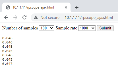
On submitting the form, we get back a raw list of values:
CSV data
Since the file we have requested is pure CSV data, that is all we get; the controls have vanished, and we’ll have to press the browser ‘back’ button if we want to retry the transaction. This is quite unsatisfactory, and to improve it there are various techniques, for example using a template system to always add the controls at the top of the data. However, we also want the browser to display the data graphically, which means a sizeable amount of Javascript, so we might as well switch to a full-blown AJAX implementation, as mentioned in the first part.
AJAX
To recap, AJAX originally stood for ‘Asynchronous JavaScript and XML’, where the Javascript on the browser would request an XML file from the server, then display data within that file on the browser screen. However, there is no necessity that the file must be XML; for simple unstructured data, CSV is adequate.
The HTML page is similar to the previous one, the main changes are that we have specified a button that’ll call a Javascript function when clicked, and there is a defined area to display the response data; this is tagged as ‘preformatted’ so the text will be displayed in a plain monospaced style.
The button calls the Javascript function ‘doSubmit’ when clicked, with the click event as an argument. As this button is in a form, by default the browser would attempt to re-fetch the current document using the form data, so we need to block this behaviour and substitute the action we want, which is to wait until the response is obtained, and display it in the area we have allocated. This is ‘asynchronous’ (using a callback function) so that the browser doesn’t stall waiting for the response.
function doSubmit() {
  // Eliminate default action for button click
  // (only necessary if button is in a form)
  event.preventDefault();

  // Create request
  var req = new XMLHttpRequest();

  // Define action when response received
  req.addEventListener( "load", function(event) {
    document.getElementById("responseText").innerHTML = event.target.responseText;
  } );

  // Create FormData from the form
  var formdata = new FormData(document.getElementById("captureForm"));

  // Collect form data and add to request
  var params = [];
  for (var entry of formdata.entries()) {
    params.push(entry[0] + '=' + entry[1]);
  }
  req.open( "GET", "/capture.csv?" + encodeURI(params.join("&")));
  req.send();
}
The resulting request sent by the browser looks something like:
GET /capture.csv?nsamples=100&xrate=1000
This is created by looping through the items in the form, and adding them to the base filename. When doing this, there is a limited range of characters we can use, in order not to wreck the HTTP request syntax. I have used the ‘encodeURI’ function to encode any of these unusable characters; this isn’t necessary with simple parameters that are just alphanumeric values, but if I’d included a parameter with free-form text, this would be needed. For example, if one parameter was a page title that might include spaces, then the title “Test page” would be encoded as
GET /capture.csv?nsamples=100&xrate=1000&title=Test%20page
You may wonder why I am looping though the form entries, when in theory they can just be attached to the HTTP request in one step:
// Insert form data into request - doesn't work!
req.open("GET", "/capture.csv");
req.send(formdata);
I haven’t been able to get this method to work; I think the problem is due to the way the browser adapts the request if a form is included, but in the end it isn’t difficult to iterate over the form entries and add them directly to the request.
The resulting browser display is a minor improvement over the previous version, in that it isn’t necessary to use the ‘back’ button to re-fetch the data, but still isn’t very pretty.
Partial display of CSV data
Graphical display
There many ways to display graphic content within a browser. The first decision is whether to use vector graphics, or a bitmap; I prefer the former, since it allows the display to be resized without the lines becoming jagged.
There is a vector graphics language for browsers, namely Scalable Vector Graphics (SVG) and I have experimented with this, but find it easier to use Javascript commands to directly draw on a specific area of the screen, known as an ‘HTML canvas’, that is defined within the HTML page:
<div><canvas id="canvas1"></canvas></div>
To draw on this, we create a ‘2D context’ in Javascript:
var ctx1 = document.getElementById("canvas1").getContext("2d");
We can now use commands such as ‘moveto’ and ‘lineto’ to draw on this context; a useful first exercise is to draw a grid across the display.
var ctx1, xdivisions=10, ydivisions=10, winxpad=10, winypad=30;
var grid_bg="#d8e8d8", grid_fg="#40f040";
window.addEventListener("load", function() {
  ctx1 = document.getElementById("canvas1").getContext("2d");
  resize();
  window.addEventListener('resize', resize, false);
} );

// Draw grid
function drawGrid(ctx) {
  var w=ctx.canvas.clientWidth, h=ctx.canvas.clientHeight;
  var dw = w/xdivisions, dh=h/ydivisions;
  ctx.fillStyle = grid_bg;
  ctx.fillRect(0, 0, w, h);
  ctx.lineWidth = 1;
  ctx.strokeStyle = grid_fg;
  ctx.strokeRect(0, 1, w-1, h-1);
  ctx.beginPath();
  for (var n=0; n<xdivisions; n++) {
    var x = n*dw;
    ctx.moveTo(x, 0);
    ctx.lineTo(x, h);
  }
  for (var n=0; n<ydivisions; n++) {
    var y = n*dh;
    ctx.moveTo(0, y);
    ctx.lineTo(w, y);
  }
  ctx.stroke();
}

// Respond to window being resized
function resize() {
  ctx1.canvas.width = window.innerWidth - winxpad*2;
  ctx1.canvas.height = window.innerHeight - winypad*2;
  drawGrid(ctx1);
}
I’ve included a function that resizes the canvas to fit within the window, which is particularly convenient when getting a screen-grab for inclusion in a blog post:
All that remains is to issue a request, wait for the response callback, and plot the CSV data onto the canvas.
var running=false, capfile="/capture.csv"

// Do a single capture (display is done by callback)
function capture() {
  var req = new XMLHttpRequest();
  req.addEventListener( "load", display);
  var params = formParams()
  req.open( "GET", capfile + "?" + encodeURI(params.join("&")));
  req.send();
}

// Display data (from callback event)
function display(event) {
  drawGrid(ctx1);
  plotData(ctx1, event.target.responseText);
  if (running) {
    window.requestAnimationFrame(capture);
  }
}

// Get form parameters
function formParams() {
  var formdata = new FormData(document.getElementById("captureForm"));
  var params = [];
  for (var entry of formdata.entries()) {
    params.push(entry[0]+ '=' + entry[1]);
  }
  return params;
}
A handy feature is to have the display auto-update when the current data has been displayed; I’ve done this by using requestAnimationFrame to trigger another capture cycle, if the global ‘running’ variable is set. Then we just need some buttons to control this feature:
The end result won’t win any prizes for style or speed, but it does serve as a useful basis for acquiring & displaying data in a Web browser.
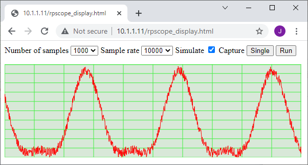
100 Hz sine wave
You’ll see that the controls have been rearranged slightly, and I’ve also added a ‘simulate’ checkbox; this invokes MicroPython code in the Pico Web server that doesn’t use the ADC; instead it uses the CORDIC algorithm to incrementally generate sine & cosine values, which are multiplied, with some random noise added:
# Simulate ADC samples: sine wave plus noise
def adc_sim():
    nsamp = parameters["nsamples"]
    buff = array.array('f', (0 for _ in range(nsamp)))
    f, s, c = nsamp/20.0, 1.0, 0.0
    for n in range(0, nsamp):
        s += c / f
        c -= s / f
        val = ((s + 1) * (c + 1)) + random.randint(0, 100) / 300.0
        buff[n] = val
    return "\r\n".join([("%1.3f" % val) for val in buff])
Distorted sine wave with random noise added
Running the code
If you haven’t done so before, I suggest you run the code given in the first and second parts, to check the hardware is OK.
Load rp_devices.py and rp_esp32.py onto the Micropython filesystem, not forgetting to modify the network name (SSID) and password at the top of that file. Then load the HTML files rpscope_capture, rpscope_ajax and rpscope_display, and run the MicroPython server rp_adc_server.py using Thonny. The files are on Github here.
You should then be able to display the pages as shown above, using the IP address that is displayed on the Thonny console; I’ve used 10.1.1.11 in the examples above.
When experimenting with alternative Web pages, I found it useful to run a Web server on my PC, as this allows a much faster development process. There are many ways to do this, the simplest is probably to use the server that is included as standard in Python 3:
python -m http.server 8000
This makes the server available on port 8000. If the Web browser is running on the same PC as the server, use the ‘localhost’ address in the browser, e.g.
http://127.0.0.1:8000/rpscope_display.html
This assumes the HTML file is in the same directory that you used to invoke the Web server. If you also include a CSV file named ‘capture.csv’, then it will be displayed as if the data came from the Pico server.
However, there is one major problem with this approach: the CSV file will be cached by the browser, so if you change the file, the display won’t change. This isn’t a problem on the Pico Web server, as it adds do-not-cache headers in the HTTP response. The standard Python Web server doesn’t do that, so will use the cached data, even after the file has changed.
One other issue is worthy of mention; in my setup, the ESP32 network interface sometimes locks up after it has transferred a significant amount of data, which means the Web server becomes unresponsive. This isn’t an issue with the MicroPython code, since the ESP32 doesn’t respond to pings when it is in this state. I’m using ESP32 Nina firmware v 1.7.3; hopefully, by the time you read this, there is an update that fixes the problem.
Copyright (c) Jeremy P Bentham 2021. Please credit this blog if you use the information or software in it.
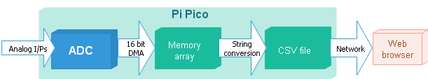
This is the second part of my Web-based Pi Pico oscilloscope project. In the first part I used an Espressif ESP32 to add WiFi connectivity to the Pico, and now I’m writing code to grab analog data from the on-chip Analog-to-Digital Converter (ADC), which can potentially provide up to 500k samples/sec.
High-speed transfers like this normally require code written in C or assembly-language, but I’ve decided to use MicroPython, which is considerably slower, so I need to use hardware acceleration to handle the data rate, specifically Direct Memory Access (DMA).
MicroPython ‘uctypes’
MicroPython does not have built-in functions to support DMA, and doesn’t provide any simple way of accessing the registers that control the ADC, DMA and I/O pins. However it does provide a way of defining these registers, using a new mechanism called ‘uctypes’. This is vaguely similar to ‘ctypes’ in standard Python, which is used to define Python interfaces for ‘foreign’ functions, but defines hardware registers, using a very compact (and somewhat obscure) syntax.
To give a specific example, the DMA controller has multiple channels, and according to the RP2040 datasheet section 2.5.7, each channel has 4 registers, with the following offsets:
The UINT32, BF_POS and BF_LEN entries may look strange, but they are just a way of encapsulating the data type, bit position & bit count into a single variable, and once that has been defined, you can easily read or write any element of the bitfield, e.g.
# Set DMA data source to be ADC FIFO
dma_chan.READ_ADDR_REG = ADC_FIFO_ADDR

# Set transfer size as 16-bit words
dma_chan.CTRL_TRIG.DATA_SIZE = 1
You may wonder why there are 2 definitions for one register: CTRL_TRIG and CTRL_TRIG_REG. Although it is useful to be able to manipulate individual bitfields (as in the above code) sometimes you need to write the whole register at one time, for example to clear all fields to zero:
# Clear the CTRL_TRIG register
dma_chan.CTRL_TRIG_REG = 0
An additional complication is that there are 12 DMA channels, so we need to define all 12, then select one of them to work on:
DMA_CHAN_WIDTH  = 0x40
DMA_CHAN_COUNT  = 12
DMA_CHANS = [struct(DMA_BASE + n*DMA_CHAN_WIDTH, DMA_CHAN_REGS)
    for n in range(0,DMA_CHAN_COUNT)]

DMA_CHAN = 0
dma_chan = DMA_CHANS[DMA_CHAN]
To add even more complication, the DMA controller also has a single block of registers that are not channel specific, e.g.
MicroPython has a function for reading the ADC, but we’ll be using DMA to grab multiple samples very quickly, so this function can’t be used; we need to program the hardware from scratch. A useful first step is to check that we can produce sensible values for a single ADC sample. Firstly the I/O pin needs to be set as an analog input, using the uctype definitions. There are 3 analog input channels, numbered from 0 to 2:
Then we clear down the control & status register, and the FIFO control & status register; this is only necessary if they have previously been programmed:
adc.CS_REG = adc.FCS_REG = 0
Then enable the ADC, and select the channel to be converted:
adc.CS.EN = 1
adc.CS.AINSEL = ADC_CHAN
Now trigger the ADC for one capture cycle, and read the result:
adc.CS.START_ONCE = 1
print(adc.RESULT_REG)
These two lines can be repeated to get multiple samples.
If the input pin is floating (not connected to anything) then the value returned is impossible to predict, but generally it seems to be around 50 to 80 units. The important point is that the value fluctuates between samples; if several samples have exactly the same value, then there is a problem.
Multiple ADC samples
Since MicroPython isn’t fast enough to handle the incoming data, I’m using DMA, so that the ADC values are copied directly into memory without any software intervention.
However, we don’t always want the ADC to run at maximum speed (500k samples/sec) so need some way of triggering it to fetch the next sample after a programmable delay. The RP2040 designers have anticipated this requirement, and have equipped it with a programmable timer, driven from a 48 MHz clock. There is also a mechanism that allows the ADC to automatically sample 2 or 3 inputs in turn; refer to the RP2040 datasheet for details.
Assuming the ADC has been set up as described above, the additional code is required. First we define the DMA channel, the number of samples, and the rate (samples per second).
The DMA destination is set to auto-increment, with a data size of 16 bits; the data request comes from the ADC. Then DMA is enabled, waiting for the first request.
Before starting the sampling, it is important to clear down the ADC FIFO, by reading out any existing samples – if this step is omitted, the data you get will be a mix of old & new, which can be very confusing.
while adc.FCS.LEVEL:
    x = adc.FIFO_REG
We can now set the START_MANY bit, and the ADC will start generating samples, which will be loaded into its FIFO, then transferred by DMA to the RAM buffer. Once the buffer is full (i.e. the DMA transfer count has been reached, and its BUSY bit is cleared) the DMA transfers will stop, but the ADC will keep trying to put samples in the FIFO until the START_MANY bit is cleared.
If you are unfamiliar with the process of loading MicroPython onto the Pico, or loading files into the MicroPython filesystem, I suggest you read my previous post.
The source files are available on Github here; you need to load the library file rp_devices.py onto the MicroPython filesystem, then run rp_adc_test.py; I normally run this using Thonny, as it simplifies the process of editing, running and debugging the code.
In the next part I combine the ADC sampling and the network interface to create a networked oscilloscope with a browser interface.
Copyright (c) Jeremy P Bentham 2021. Please credit this blog if you use the information or software in it.
Analog to Digital Converter (ADC) driver software usually captures a single block of samples; if a larger dataset (or continuous stream) is required, it can be very difficult to merge multiple blocks without leaving any gaps.
In this post I describe a utility that runs from the command-line, and performs continuous data capture to a Linux First In First Out (FIFO) buffer, that can be accessed by another Pi program, written in any language. The software also captures a microsecond time-stamp for each data block, that can be used to validate the timing, making sure there are no gaps.
To achieve this performance, I’m heavily reliant on Direct Memory Access (DMA) as described in a previous post; if you are a newcomer to the technique, I suggest you experiment with that code first, since it is much simpler.
ADC hardware
AB Electronics ADC DAC Zero on a Pi 3B
For this demonstration I’m using the ‘ADC-DAC Pi Zero’ from AB Electronics; despite the name, it is compatible with the full range of RPi boards. It uses an MCP3202 12-bit ADC with 2 analog inputs, measuring 0 to 3.3 volts at up to 60K samples per second. It also has 2 analog outputs from an MCP4822 DAC; I had planned to include these in the current software, but ran out of time – they may well feature in a future post.
As is common with mid-range ADC boards, it uses the Serial Peripheral Interface zero (SPI0) for data transfers. It has a 4-wire interface (plus ground) comprising transmit & receive data, a clock line, and Chip Enable zero (CE0).
ADC serial protocol
To get a sample from the ADC, it is necessary to drive the Chip Enable (CE) line low, clock in a command, clock out the data, and drive CE high. The SPI clock signal isn’t just used for data transmission, it also controls the internal logic of the ADC, so there is a limit on how fast it can be toggled; the data sheet is a bit vague on this subject (only specifying a limit of 1.8 MHz with 5V supply, and 0.9 MHz with 2.7V), so I’ve used a conservative value of 1 MHz. The data format is a 4-bit command, a null bit, and 12-bit response, making an awkward size of 17 bits. My software ignores the least-significant bit, so uses more convenient 16-bit transfers, with a maximum rate of 60K samples/sec. The command and response format is:
COMMAND:
  Start bit:                 1
  Single-ended mode          1
  Channel number             0 or 1
  M.S. bit first             1
  Dummy bits for response    0 0 0 0 0 0 0 0 0 0 0 0

RESPONSE:
  Undefined bits (floating)  x x x x
  Null bit                   0
  Data bits 11 to 0          x x x x x x x x x x x x
So the command for channel 0 is D0 hex, channel 1 is F0 hex. The following oscilloscope trace shows 2 transfers at 50,000 samples per second; you can see that the CE line goes low one clock cycle before the start of the transaction, and goes high on the last clock edge. This is because I’ve used the automatic-CE capability of the SPI interface, which provides very accurate timings.
ADC readings on a Pi Zero
The voltage is calculated by taking the value from the lower 11 bits, multiplying by the reference voltage, and dividing by the full-scale value, so 0x2AC * 3.3 / 2048 = 1.102 volts.
Raspberry Pi SPI
The SPI controller has the following 32-bit registers:
CS (control & status): configuration settings, and status information
FIFO (first-in-first-out): 16-word buffers for transmit & receive data
CLK (clock divisor): set the clock rate of the SPI interface
DLEN (data length): the transmit/receive length in bytes (see below)
LTOH (LOSSI output hold delay): not used
DC (DMA configuration): set the trigger levels for DMA data requests
The bit fields within these registers are described in the BCM2835 ARM Peripherals document available here, and the errata here; I’ll be concentrating on aspects that aren’t fully described in that document.
CS bits 0 & 1: select chip enable. The terms Chip Enable (CE) and Chip Select (CS) are used interchangeably to describe the hardware line that enables communication with the ADC or DAC chip, but CS is confusing as there is a CS (Control & Status) register as well, so I prefer to use CE. Bits 0 & 1 of that register control which CE line is used; the ADC is on CE0, and the DAC is on CE1.
CS bits 4 & 5: Tx and Rx FIFO clear. When debugging, it is quite common for there to be data left in the FIFOs, so it is a good idea to clear the FIFOs on startup.
CS bit 7: transfer active. When in DMA mode, set this bit to enable the SPI interface for data transfers. The transfer will start when there is data to be transmitted in the FIFO; after the specified length of data has been transferred, this bit will be cleared.
CS bit 8: DMAEN. This does not enable DMA, it just configures the SPI interface to be more DMA-friendly, as I’ll describe below. It isn’t necessary to use DMA when DMAEN is set; when trying to understand how this mode works, I used simple polled code.
CS bit 11: automatically deassert chip select. When set, the SPI interface can automatically frame each 16-bit transfer with the CE line; setting it low before the start, and high at the end, as shown in the oscilloscope trace above.
There is a confusing interaction between Transfer Active bit (TA), and the Data Length register (DLEN). Basically there are 2 very different ways of setting the data length at the start of a transfer:
If TA is clear, the length (in bytes) must first be set in the DLEN register. Then TA is set, and the transaction will start when there is data in the transmit FIFO.
If TA is set, the DLEN register is ignored. The length (in bytes) must first be written into the FIFO, together with some of the CS register settings, then the transfer will start when data is written to the transmit FIFO.
I generally use the first method, but either is workable providing you have a clear idea of the whether the transfer is active or not – don’t forget that it is automatically cleared when the length becomes zero.
An additional complication comes from the fact that DMA transfers and FIFO registers are 4 bytes wide, but we’re only doing 2-byte transfers to the ADC. The remaining 2 bytes aren’t automatically discarded; they stay in the FIFO to be used by the next transaction. It is possible to use this fact, and economise on memory by having 2 transmit words in one 4-byte memory location, but this can get really confusing (particularly with method 2) so I use a clear-FIFO command in each transfer to remove the extra. This means that the transmit & receive data only uses 16 bits in every 32-bit word.
SPI, PWM and DMA initialisation
To initialise the SPI & PWM controllers, we need to know what master clock frequency they are getting, in order to calculate the divisor values that’ll produce the required output frequencies. The frequencies (in MHz) depend on which Pi hardware version we’re using:
The channel usage was determined by running my rpi_disp_dma utility, and the PWM & SPI clock values were checked using the rpi_adc_stream application in test mode, as described later in this post.
Sadly, this table isn’t telling the whole truth with regard to the values for SPI master clock. These are the values in normal operation, however if the CPU temperature is too high, its clock frequency is scaled back, and so is the SPI master clock. Mercifully the PWM frequency remains constant, so the sample rate of our code is unaffected, but as you’ll see from the oscilloscope trace above, if we’re running at 50K samples per second, there isn’t a lot of spare time, so if the SPI clock slows down, the transfers could fail to complete, causing garbage data and/or DMA timeouts.
This will only be a problem if you’re working close to the maximum sample rate, and if necessary, there are various workarounds you can use; for example, increase the SPI frequency, since the ADC does seem to tolerate values greater then 1 MHz, or fix the CPU clock frequency by changing the settings in /boot/config.txt.
The table also includes a list of active DMA channels, obtained by my rpi_disp_dma utility, as described later. Based on this result, I generally use channels 7, 8 & 9 in my code but of course there is no guarantee these will remain unused in any future OS release. If in doubt, run the utility for yourself.
Using DMA
The only way of getting ADC samples at accurately-controlled intervals is to use Direct Memory Access (DMA). Once set up, this acts completely independently of the CPU, transferring data to & from the SPI interface. We probably don’t want to run the ADC flat out, so need a method of triggering it after a specific time delay. In the absence of any hardware timers (surprisingly, the RPi CPU doesn’t have any conventional counter/timers) we’re using the Pulse Width Modulation (PWM) interface for timed triggering (which is generally known as ‘pacing’).
So we need to set up 3 DMA channels; one for transmit data, one for receive data, and one for pacing. I’ve tried to make the process of doing this as simple as possible, with a very clean structure. The DMA Control Blocks (CBs) and data must be in un-cached memory, as described in my previous post, so I’ve simplified the program steps to:
Prepare the CBs and data in user memory.
Copy the CBs and data across to uncached memory
Start the DMA controllers
Start the DMA pacing
To keep the organisation of the variables very clear, they are in a structure that can be overlaid onto both the user and the uncached memory. Here is the code for steps 1 and 2:
The initialised values are assembled in dma_data, then copied into uncached memory at dp. The control blocks are at the start of the structure, to be sure they’re aligned to the nearest 32-byte boundary. Then there is the data to be transmitted, and some storage for the timestamps, that is marked as ‘volatile’ since it will be modified by DMA.
The format of a control block is:
Transfer Information (TI): address increment, trigger signal (data request), etc.
Source address
Destination address
Transfer length (in bytes)
Stride: skip unused values (not used)
Next Control Block: zero if last block
Debug: additional diagnostics
Looking at the first control block (CB 0) in detail:
#define SPI_RX_TI       (DMA_SRCE_DREQ | (DMA_SPI_RX_DREQ << 16) | DMA_WAIT_RESP | DMA_CB_DEST_INC)

{SPI_RX_TI, REG(usec_regs, USEC_TIME), MEM(mp, &dp->usecs[0]),  4, 0, CBS(1), 0}, // 0

Transfer info:       wait for data request from SPI receiver
Source address:      microsecond counter register
Destination address: memory
Transfer length:     4 bytes
Stride:              not used
Next control block:  CB 1
Debug:               not used
The source and destination addresses are more complex than usual, since they must be bus address values, created using a macro that takes a pointer to a block of mapped memory, and the offset within that block.
For this application, we need to keep re-transmitting the same bytes to request the data, but reception is in the form of long blocks of data; I’ve specified 2 blocks, that form a ‘ping-pong’ buffer, with the microsecond timestamp being stored at the start of each block, and a completion flag at the end. Ideally, the user code will be emptying one buffer while the other is being filled by DMA, but if the code is too slow, the overrun condition can be detected, and the data discarded.
Starting DMA
When we start the 3 DMA channels, they will all remain idle until the condition specified in TI is fulfilled:
To set the data-gathering in motion, we just enable PWM.
// Start ADC data acquisition
void adc_stream_start(void)
{
    start_pwm();
}
This sends a data request, which is fulfilled by DMA channel A (CB7), and nothing else happens; the SPI interface remains idle. However, on the next PWM timeout, CBS 8 & 9 are executed, which loads a value of 2 into the DLEN register, and sets the SPI transfer active. This triggers a request for Tx data from DMA channel C (CB6); when the first 2 bytes have been transferred, DMA channel B is triggered to store the microsecond timestamp (CB0), and the data (CB1). Since the transfer is no longer active, the DMA channels will all wait for their trigger signals, and the cycle will repeat, except that CB1 is storing the incoming ADC data in a single block.
Once the required number of samples have been received, CB2 sets a flag to indicate the buffer is full, then CB4 starts filling the other buffer.
Compiling and running the code
The C source code for the streaming application rpi_adc_stream and the DMA detection application rpi_disp_dma are on github here. You’ll also need the utility files rpi_dma_util.c and rpi_dma_util.h from the same directory.
Edit the top of rpi_dma_util.h to indicate which hardware version you are using (0 to 4, or 2 for the Zero2). The applications are compiled using a minimal command line:
There is only one command line option, ‘-v’ for verbose operation, which prints out all the DMA register values.
By default, DMA_CHAN_A, B and C are defined in rpi_dma_utils.h as channels 7, 8 and 9, so should not conflict with those used by the OS.
ADC streaming
There are various command-line options, but it is suggested that you start by using the -t option to check the SPI and PWM interfaces are running correctly:
A small error in the reading (e.g. 100.010 Hz) doesn’t indicate a fault, it is just due to the limited resolution of the timer that is making the measurement.
The command-line options are case-insensitive:
-F <num>    Output format, default 0. Set to 1 to enable microsecond timestamps.
-I <num>    Number of input channels, default 1. Set to 2 if both channels required.
-L          Lockstep mode. Only output streaming data when the Linux FIFO is empty.
-N <num>    Number of samples per block, default 1.
-R <num>    Sample rate, in samples per second, default 100.
-S <name>   Enable streaming mode, using the given FIFO name.
-T          Test mode
-V          Verbose mode. Enable hexadecimal data display.
Running the utility with no arguments will perform a single conversion on the first ADC channel (marked ‘IN1’):
Command:
  sudo ./rpi_adc_stream
Response:
  RPi ADC streamer v0.20
  VC mem handle 5, phys 0xde50f000, virt 0xb6fd1000
  SPI frequency 1000000 Hz
  ADC value 686 = 1.105V
  Closing
If the input isn’t connected to anything, you will get a random result; either short-circuit the input pins, or connect them to a known voltage source (less than 3.3V) to get a proper reading.
To stream the voltage values, it is necessary to specify the number of samples per block, the sample rate, and a Linux FIFO name; you can choose (almost) any name you like, but it is recommended to put the FIFO in the /tmp directory, e.g.
Command:
  sudo ./rpi_adc_stream -n 10 -r 20 -s /tmp/adc.fifo
Response:
  RPi ADC streamer v0.20
  VC mem handle 5, phys 0xde50f000, virt 0xb6f7e000
  Created FIFO '/tmp/adc.fifo'
  Streaming 10 samples per block at 20 S/s
The software is now waiting for another application to open the Linux FIFO, before it will start streaming. The FIFO is very similar to a conventional file, so some of the standard file utilities can be used, e.g. ‘cat’ to print the file. Open a second Linux console, and in it type:
Command:
  cat /tmp/adc.fifo
Response (with 1.1V on ADC 'IN1'):
  1.102,1.104,1.104,1.102,1.104,1.104,1.110,1.104,1.102,1.102
  1.105,1.104,1.104,1.104,1.105,1.102,1.102,1.104,1.104,1.104
  ..and so on, at 2 blocks per second..
Hit ctrl-C to stop this command, and you’ll see that the streamer can detect that there is nothing reading the FIFO, so reports ‘stopped streaming’, though it does continue to fetch data using DMA, since this has minimal impact on any other applications.
You’ll note that it hasn’t been necessary to run the data display command using ‘sudo’; it works fine from a normal user account. It is important to limit the amount of code that has to run with root privileges, and the Linux FIFO interface is a handy way of achieving this.
There is a ‘-f’ format option, that controls the way the data is output. Currently there is only one possibility ‘-f 1’ which enables a microsecond timestamp on each block of data, e.g.
Command in console 1:
  sudo ./rpi_adc_stream -n 1 -r 10 -f 1 -s /tmp/adc.fifo
Response:
  Streaming 1 samples per block at 10 S/s

Command in console 2:
  cat /tmp/adc.fifo
Response in console 2 (with 1.1 volt input):
  0,1.102
  100000,1.104
  200000,1.102
  300001,1.105
  400001,1.104
  ..and so on, at 10 lines per second
The timestamp started at zero, then incremented by 100,000 microseconds every block. It is a 32-bit number, so if you want to measure times longer than 7 minutes, you will need to detect when the value has wrapped around.
If 2 input channels are enabled using ‘-i 2’, then the overall sample rate remains unchanged, each channel has half the samples. In the following example, I’ve also enabled verbose mode, to see the ADC binary data:
Command in console 1:
  sudo ./rpi_adc_stream -n 2 -i 2 -r 10 -f 1 -s /tmp/adc.fifo -v
Response in console 1:
  Streaming 2 samples per block at 10 S/s
Response when streaming starts:
  Started streaming to FIFO '/tmp/adc.fifo'
  F2 AD 00 00 F0 01 00 00
  F2 AE 00 00 F0 01 00 00
  F2 AE 00 00 F0 01 00 00
  F2 AE 00 00 F0 00 00 00
  ..and so on..

Command in console 2:
  cat /tmp/adc.fifo
Response in console 2 (IN1 is 1.1 volts, IN2 is zero):
  1.104,0.002
  1.105,0.002
  1.105,0.002
  1.105,0.000
  ..and so on..
Displaying streaming data
It’d be nice to view the streaming data in a continually-updated graph, similar to an oscilloscope display, but surprisingly few graphing utilities can handle a continuous flow of data – or they can only handle it at a very low rate.
Here are a few graphing utilities I’ve tried; they perform reasonably well on fast hardware, but struggle to maintain a good-quality graph on slower boards such as the Pi Zero – there is no problem with the data acquisition, it is just that the graphical display is very demanding.
Trend display
There is a Linux utility called ‘trend’, that can dynamically plot streaming data.
Trend display of a 50 Hz analog signal, 5000 samples per second
It has a wide range of options, and keyboard shortcuts, that I haven’t yet explored. The above graph was generated on a Pi 4 using the following command in one console:
This application is quite demanding on CPU resources, so if you are using a Pi 3, you’ll probably need to drop the sample rate to 2000.
Termeter display
Termeter is a really useful text-based dynamic display utility, written in the Go language.
You may wonder why I’m using a text-based console application to produce a graph, but it has two key advantages; it is very fast, and works on any Pi console. So if you are running the Pi ‘headless’ (i.e. remotely, with no local display) and you want to look your streaming data, you can run termeter on a remote console (e.g. ‘putty’ on windows) without the complexity of setting up an X display server.
It is installed using:
cd ~
sudo apt install golang
go get github.com/atsaki/termeter/cmd/termeter
The above data (1 sample per block, 5000 samples per second) was generated on a Pi 4 by running in one console:
On a Pi 3, you might have to drop the sample rate to 2000, and even further on a Pi Zero.
Plotting in Python
Python plot of streaming data
Here is a very simple example that uses NumPy and Matplotlib to create a dynamically-updated graph of ADC data (a 10 Hz sine wave, at 200 samples per second, on a Pi 4). In one terminal, the data is generated by running:
The ‘readline’ function fetches a single line of comma-delimited data, which ‘fromstring’ converts to a NumPy array.
The ‘animate’ function is used to continuously refresh the graph, however this approach is only suitable for low update rates; the time taken to do the plot is quite significant, and there is an inherent conflict between the data rate set by the streamer, and the display rate set by the animation, causing the display to stall, especially on a single-core Pi Zero. A multi-threaded program is needed to coordinate the display updates with the incoming data.
Update
The display problem has been solved by creating a fast oscilloscope-type viewer for the streaming data, using OpenGL.
WebGL oscilloscope display
Full details and source code are here, and there is a WebGL version that works remotely in a browser here.
Copyright (c) Jeremy P Bentham 2020. Please credit this blog if you use the information or software in it.
The Secondary Memory Interface (SMI) is a parallel I/O interface that is included in all the Raspberry Pi versions. It is rarely used due to the acute lack of publicly-available documentation; the only information I can find is in the source code to an external memory device driver here, and an experimental IDE interface here.
However, it is a very useful general-purpose high-speed parallel interface, that deserves wider usage; in this post I’m testing it with digital-to-analogue and analogue-to-digital converters (DAC and ADC) but there are many other parallel-bus devices that would be suitable.
To take advantage of the high data rates, I’ll be using the C language, and Direct Memory Access (DMA); if you are unfamiliar with DMA on the RPi, I suggest you read my previous 2 posts on the subject, here and here.
Parallel interface
Raspberry Pi SMI signals
The SMI interface has up to 18 bits of data, 6 address lines, read & write select lines. Transfers can be initiated internally, or externally via read & write request lines, which can take over the uppermost 2 bits of the data bus. Transfer data widths are 8, 9, 16 or 18 bits, and are fully supported by First In First Out (FIFO) buffers, and DMA; this makes for efficient memory usage when driving an 8-bit peripheral, since a single 32-bit DMA transfer can automatically be converted into four 8-bit accesses.
If you have ever worked with the classic bus-interfaces of the original microprocessors, you’ll feel quite at home with SMI, but no need to worry about timing problems, because the setup, strobe & hold times are fully programmable with 4 nanosecond resolution; what luxury!
The SMI functions are assigned to specific GPIO pins:
The GPIO pins to be included in the parallel interface are selected by setting their mode to ALT1; there is no requirement to set all the SMI pins in this way, so the I2C, SPI and PWM interfaces are still quite usable.
Parallel DAC
Hardware
The simplest device to drive from the parallel bus is a digital-to-analogue converter (DAC), using resistors from each data line to a common output. This arrangement is commonly known as an R-2R ladder, due to the resistor values needed.
I’ve used a pre-built device from Digilent (details here, or newer version here) but it is easy to make your own using discrete resistors; the least-significant is connected to GPIO8 (SD0), and the most-significant to GPIO15 (SD7).
Software
I’ll be making extensive use of the dma_utils functions that were created for my previous DMA projects, but before diving into the complication of SMI, it is helpful to test the hardware using simpler GPIO commands:
This is less-than-ideal because we have to use one command to set some I/O pins to 1, and another command to clear the rest to 0, so in the gap between them the I/O state will be incorrect; also we won’t get accurate timing with the usleep command.
To my surprise, when I ran this code on a Pi Zero, and viewed the output on an oscilloscope, it didn’t look too bad; however, as soon as I moved the mouse, there were very significant gaps in the output, so clearly we need to do better.
SMI register definitions
To use SMI, we first need to define the control registers, and the bit-values within them. The primary reference is bcm2835_smi.h from the Broadcom external memory driver, but I found this difficult to use in my code, so converted the definitions into C bitfields; this makes the code a bit less portable, but a lot simpler and easier to read.
Also, when learning about a new peripheral, it is helpful if the bitfield values can be printed on the console. This normally requires the tedious copying of register field names into string constants, but with a small amount of macro processing, this can be done with a single definition, for example the SMI CS register:
The last bit of code is needed so that smi_cs points to the register in virtual memory; if you don’t understand why, I suggest you read my post on RPi DMA programming here. Anyway, the upshot of all this code is that we can access the whole 32-bit value of the register as smi_cs->value, and also individual bits such as smi_cs->enable, smi_cs->done, etc.
To print out the bit values, we use macros to convert the register definition to a string, then have a simple C parser:
#define STRS(x)     STRS_(x) ","
#define STRS_(...)  #__VA_ARGS__

char *smi_cs_regstrs = STRS(SMI_CS_FIELDS);

// Display bit values in register
void disp_reg_fields(char *regstrs, char *name, uint32_t val)
{
    char *p=regstrs, *q, *r=regstrs;
    uint32_t nbits, v;

    printf("%s %08X", name, val);
    while ((q = strchr(p, ':')) != 0)
    {
        p = q + 1;
        nbits = 0;
        while (*p>='0' && *p<='9')
            nbits = nbits * 10 + *p++ - '0';
        v = val & ((1 << nbits) - 1);
        val >>= nbits;
        if (v && *r!='_')
            printf(" %.*s=%X", q-r, r, v);
        while (*p==',' || *p==' ')
            p = r = p + 1;
    }
    printf("\n");
}
Now we can display all the non-zero bit values using:
CS:  control and status
L:   data length (number of transfers)
A:   address and device number
D:   data FIFO
DMC: DMA control
DSR: device settings for read
DSW: device settings for write
DCS: direct control and status
DCA: direct control address and device number
DCD: direct control data
You can specify up to 4 unique timing settings for read & write, making 8 settings in total. The settings are specified by giving a 2-bit device number for each transaction; this selects 1 of the 4 descriptors for read or write. I’ve only used one pair of settings, and the ADC & DAC don’t have address lines, so the address & device register remains at zero.
Direct mode is a simple way of doing accesses using the appropriate timings, but without DMA; it has separate address, data and control registers.
Some notable fields in the control & status register are:
Enable: it is obvious that this bit must be set for SMI to work, but it is less obvious when that should be done. Initially, I assumed it was necessary to enable the interface before any other initialisation, but then it responded with the ‘settings error’ bit set. So now I do most of the configuration with the device disabled, then enable it before clearing the FIFOs and enabling DMA, otherwise the transfers go through immediately.
Start: set this bit to start the transfer; the SMI controller will perform the number of transfers in the length register, using the timing parameters specified in DSR (for read) or DSW (for write). If there is a backlog of data (FIFO is full) the transaction may stall.
Pxldat: when this ‘pixel data’ bit is set, the 8- or 16-bit data is packed into 32-bit words.
Pvmode: I have no idea what this ‘pixel valve’ mode should do; any information would be gratefully received.
Direct Mode
As the name implies, SMI Direct Mode allows you to perform a single I/O transfer without DMA. However, it is still necessary to specify the timing parameters of the transfer, specifically:
The clock period, that will be used for the following timing:
The setup time, that is used by the peripheral to decode the address value
The width of the strobe pulse, that triggers the transfer
The hold time, that keeps the signals stable after the transfer
To add to the complication, the SMI controller can drive 4 peripheral devices, each with its own individual read & write settings, so there are a total of 8 timing registers. I’m keeping this simple by always using the first register pair (for device zero) but it is worth remembering that you can define more than one set of timings, and quickly switch between them by setting the device number.
Likewise, I’m ignoring the address field since it is also redundant for my DAC; for safety, I clear all the SMI registers on startup, in case there are any residual unwanted values.
As it happens, this setup/strobe/hold timing is largely redundant for our simple resistor DAC (since it doesn’t latch the data) but we still need to specify something, for example if we want the overall cycle time to be 1 microsecond, this can be achieved with a clock period of 10 nanoseconds, setup 25, strobe 50, and hold 25, since (25 + 50 + 25) * 10 = 1000 nanoseconds. This is the code I use to set the timing:
// Width values
#define SMI_8_BITS  0
#define SMI_16_BITS 1
#define SMI_18_BITS 2
#define SMI_9_BITS  3

// Initialise SMI interface, given time step, and setup/hold/strobe counts
// Clock period is in nanoseconds: even numbers, 2 to 30
void init_smi(int width, int ns, int setup, int strobe, int hold)
{
    int divi = ns/2;

    smi_cs->value = smi_l->value = smi_a->value = 0;
    smi_dsr->value = smi_dsw->value = smi_dcs->value = smi_dca->value = 0;
    if (*REG32(clk_regs, CLK_SMI_DIV) != divi << 12)
    {
        *REG32(clk_regs, CLK_SMI_CTL) = CLK_PASSWD | (1 << 5);
        usleep(10);
        while (*REG32(clk_regs, CLK_SMI_CTL) & (1 << 7)) ;
        usleep(10);
        *REG32(clk_regs, CLK_SMI_DIV) = CLK_PASSWD | (divi << 12);
        usleep(10);
        *REG32(clk_regs, CLK_SMI_CTL) = CLK_PASSWD | 6 | (1 << 4);
        usleep(10);
        while ((*REG32(clk_regs, CLK_SMI_CTL) & (1 << 7)) == 0) ;
        usleep(100);
    }
    if (smi_cs->seterr)
        smi_cs->seterr = 1;
    smi_dsr->rsetup = smi_dsw->wsetup = setup;
    smi_dsr->rstrobe = smi_dsw->wstrobe = strobe;
    smi_dsr->rhold = smi_dsw->whold = hold;
    smi_dsr->rwidth = smi_dsw->wwidth = width;
}
The clock-frequency-setting code is similar to that I used to set the PWM frequency for my DMA pacing; that peripheral did seem to be really sensitive to any glitches in the clock, so I’ve been a bit over-cautious in adding extra time-delays, which may not really be necessary.
The seterr flag is supposed to indicate an error if the settings have been changed while the SMI device is active; the easiest way to avoid this error is to do most of the settings while the device is disabled, then enable it just before starting; the flag is also cleared on startup, by writing a 1 to it.
Once the timing is set, the following code can be used to initiate a single direct-control write-cycle:
The code clears the FIFO, in case there is any data left over from a previous transaction (which isn’t unusual, if you have been using DMA), and the FIFO error flag, then enables the device. The transfer is initiated by clearing the completion flag, setting write mode, loading the value into the Direct Mode data register, then starting the cycle.
The transfer then proceeds using the specified timing, and the completion flag is set when complete. If we run this code with usleep for timing, there is very little difference in the DAC output; it is still susceptible to other events, such as mouse movement, as shown in the oscilloscope trace below.
To gain maximum benefit from SMI, we have to use DMA.
SMI and DMA
When using SMI with DMA, the fundamental question is where the DMA requests will be coming from.
They can be triggered by an external signal, in ‘DMA passthrough’ mode. The data lines SD 16 & 17 can be used as triggers; SD16 to write to an external device or SD17 to read from external device, with a maximum data width of 16 bits. It is important to note that they are level-sensitive signals (not edge-triggered) so if held high, the transfers will carry on at the maximum rate; see the oscilloscope trace below, where a 500 ns request is sufficient to trigger 2 transfers.
Oscilloscope trace of DMA passthrough (200 ns/div)
So DMA passthrough is designed for use with peripherals that assert the request when they have data to send, and negate it when the transfer has gone through. I have experimented with the PWM controller to generate narrow pulses, and it does seem possible to trigger single transfers this way, but more tests are needed to make sure this method is 100% reliable, so for the time being I won’t use it.
Instead, the requests will originate from the SMI controller itself; the transfer will proceed at the maximum speed defined by the setup, strobe & hold times, with DMA keeping the FIFOs topped up with data. This places a lower limit on the rate at which the transfers go through; the maximum clock resolution is 30 ns, and the maximum setup, strobe & hold values are 63, 127 and 63, giving a slowest cycle time of 7.6 microseconds.
The DMA Control Block is similar to those in my previous projects; it just needs a data source in uncached memory, data destination as the SMI FIFO, and length
A convenient way of outputting a repeating waveform is to create one cycle in memory, and set the control block to that length. Then the SMI length is set to the total number of bytes to be sent, assuming the pixel mode flag ‘pxldat’ has been set; this instructs the SMI controller to unpack the 32-bit DMA & FIFO values into 4 sequential output bytes.
The following trace was generated by a 256-byte ramp, repeated 6 times, using a 1 microsecond cycle time.
Oscilloscope trace of DAC output (200 us/div)
The SMI interface can generate much faster waveforms, but unfortunately they aren’t rendered very well by the DAC as it uses 10K resistors; when these are combined with the oscilloscope probe input capacitance, the resulting rise time is around 500 nanoseconds. So for faster waveforms, you need a faster DAC.
Read cycle test
The last DAC test I’m going to do will seem a bit crazy: a read cycle. The settings are the same as the write-cycle, with the following changes:
The scope has been set to additionally show the SOE signal as the top trace:
The DAC output starts at 3.3V which was the final value of the previous output cycle. It then drops to 1.2V during the read cycles, as this is the value it floats to when the I/O lines aren’t being driven. At the end of the last read cycle, the output is driven back to 3.3V.
This is a very important result; as soon as the input cycles stop, SMI drives the bus. This is because memory chips don’t like a floating data bus; a halfway-on voltage can cause excessive power dissipation, and even damage the chip in extreme cases. So it is a sensible precaution that the data bus is always driven, though this is about to cause a major problem…
AD9226 ADC
Searching the Internet for a fast low-cost analogue-to-digital (ADC) module with a parallel interface, I found very few; the best one featured the 12-bit AD9226, with a maximum throughput of 65 megasamples per second. It requires a 5 volt supply, but has a 3.3V logic interface, so is compatible with the Raspberry Pi.
Having worked with the module for a few days, I’ve found it to be less than ideal, for various reasons that’ll be given later, but it is still useful to demonstrate high-speed parallel input with SMI.
Connecting to the RPi isn’t difficult, but as we’re dealing with high-speed signals, it is necessary to keep the wiring short, preferably under 50 mm (2 inches), especially the power, ground & clock signals.
One minor confusion is that the pin marked D0 is the most-significant bit, and D11 the least significant; I wanted to leave the SPI0 pins free, so adopted the following connection scheme, which puts the data in the top 12 bits of a 16-bit SMI read cycle.:
We’ll start by using Direct Mode to obtain an sample without DMA. The ADC is designed to work with a continuous clock signal, but ours is derived from the SMI Output Enable (OE) line, so only changes state during data transfers.
The AD9226 data sheet describes how it stabilises the clock signal, and suggests it may require over 100 cycles when adapting to a new frequency. In practice, when starting up there seems to be a major data glitch after 8 cycles, but after that the conversions appear to have stabilised, so I allow for 10 cycles before taking a reading.
It is necessary to choose timing values for the SMI cycles; my default settings are 10 nanosecond time interval, with a setup of 25, strobe 50, hold 25, so the total cycle time is 10 * (25 + 50 + 25) = 1000 nanoseconds, or 1 megasample/sec.
The ADC has an op-amp input circuit that can accommodate positive and negative voltages. Converting the ADC value to a voltage is a bit fraught; I determined the following values by experimentation with one module, but suspect they are subject to quite wide component tolerances, so won’t be the same for all modules.
#define ADC_ZERO        2080
#define ADC_SCALE       410.0

// Convert ADC value to voltage
float val_volts(int val)
{
    return((ADC_ZERO - val) / ADC_SCALE);
}

// Return ADC value, using GPIO inputs
int adc_gpio_val(void)
{
    int v = *REG32(gpio_regs, GPIO_LEV0);

    return((v>>ADC_D0_PIN) & ((1 << ADC_NPINS)-1));
}
It is important to note that the module has a 50-ohm input, so imposes a very heavy loading on any circuit it is monitoring. It can’t cope with significant voltages for any period of time; for example, if you apply 5 volts, the input resistor will dissipate half a watt, heat up rapidly, and probably burn out.
So, although the ADC is excellent for fast data acquisition, the module isn’t really suitable for general purpose measurement, and would benefit from a redesign with a high-impedance input.
Avoiding bus conflicts
The module doesn’t have a chip-select or chip-enable input, so the data is always being output; the 28-pin version of the AD9226 doesn’t have the facility for disabling its output drivers. In the above code I avoided the possibility of bus conflicts doing a GPIO register read, but for high speeds we have to use SMI read cycles. This is potentially a major problem; when the read cycles are complete, the SMI controller and the ADC will both try to drive the data bus at the same time, causing significant current draw, only limited by the 100 ohm resistors on the module: they are insufficient to keep the current below the maximum values (16 mA per pin, 50 mA total for all I/O) in the Broadcom data sheet.
I’ve experimented with various software solutions, basically using a DMA Control Block to set the ADC pins to SMI mode (ALT1), then the second CB for the data transfer, then a third to set the pins back to GPIO inputs. The problem with this approach is that at the higher transfer rates the DMA controller is only just keeping up with the incoming data, and there is a sizeable backlog that has to be cleared before the DMA completes. So there is a significant delay before the SMI pins are set back to inputs, and in that time, there is a bus conflict.
For this reason (and to avoid any concerns about hardware damage when debugging new code) I added a resistor in series with each data line, to reduce the current flow when a bus conflict occurs. The value is a compromise; the resistance needs to be high enough to block excessive current, but not so high that it will slow down the I/O transitions too much, when combined with the stray capacitance of the GPIO inputs.
I chose 330 ohms, which combines with the 100 ohms already on the module, to produce a maximum current of 7.7 mA per line. This is well within the per-pin limit of the Broadcom device, but if all the lines are in conflict, the total will actually exceed the maximum chip I/O current, so it is inadvisable to leave the hardware in this state for a significant period of time.
ADC code
If you’ve read my previous blogs on fast ADC data capture, the DMA code will seem quite familiar, with control blocks to set the GPIO pins to SMI mode, capture the data, and restore the pins:
// Get GPIO mode value into 32-bit word
void mode_word(uint32_t *wp, int n, uint32_t mode)
{
    uint32_t mask = 7 << (n * 3);
    *wp = (*wp & ~mask) | (mode << (n * 3));
}

// Start DMA for SMI ADC, return Rx data buffer
uint32_t *adc_dma_start(MEM_MAP *mp, int nsamp)
{
    DMA_CB *cbs=mp->virt;
    uint32_t *data=(uint32_t *)(cbs+4), *pindata=data+8, *modes=data+0x10;
    uint32_t *modep1=data+0x18, *modep2=modep1+1, *rxdata=data+0x20, i;

    // Get current mode register values
    for (i=0; i<3; i++)
        modes[i] = modes[i+3] = *REG32(gpio_regs, GPIO_MODE0 + i*4);
    // Get mode values with ADC pins set to SMI
    for (i=ADC_D0_PIN; i<ADC_D0_PIN+ADC_NPINS; i++)
        mode_word(&modes[i/10], i%10, GPIO_ALT1);
    // Copy mode values into 32-bit words
    *modep1 = modes[1];
    *modep2 = modes[2];
    *pindata = 1 << TEST_PIN;
    enable_dma(DMA_CHAN_A);
    // Control blocks 0 and 1: enable SMI I/P pins
    cbs[0].ti = DMA_SRCE_DREQ | (DMA_SMI_DREQ << 16) | DMA_WAIT_RESP;
    cbs[0].tfr_len = 4;
    cbs[0].srce_ad = MEM_BUS_ADDR(mp, modep1);
    cbs[0].dest_ad = REG_BUS_ADDR(gpio_regs, GPIO_MODE0+4);
    cbs[0].next_cb = MEM_BUS_ADDR(mp, &cbs[1]);
    cbs[1].tfr_len = 4;
    cbs[1].srce_ad = MEM_BUS_ADDR(mp, modep2);
    cbs[1].dest_ad = REG_BUS_ADDR(gpio_regs, GPIO_MODE0+8);
    cbs[1].next_cb = MEM_BUS_ADDR(mp, &cbs[2]);
    // Control block 2: read data
    cbs[2].ti = DMA_SRCE_DREQ | (DMA_SMI_DREQ << 16) | DMA_CB_DEST_INC;
    cbs[2].tfr_len = (nsamp + PRE_SAMP) * SAMPLE_SIZE;
    cbs[2].srce_ad = REG_BUS_ADDR(smi_regs, SMI_D);
    cbs[2].dest_ad = MEM_BUS_ADDR(mp, rxdata);
    cbs[2].next_cb = MEM_BUS_ADDR(mp, &cbs[3]);
    // Control block 3: disable SMI I/P pins
    cbs[3].ti = DMA_CB_SRCE_INC | DMA_CB_DEST_INC;
    cbs[3].tfr_len = 3 * 4;
    cbs[3].srce_ad = MEM_BUS_ADDR(mp, &modes[3]);
    cbs[3].dest_ad = REG_BUS_ADDR(gpio_regs, GPIO_MODE0);
    start_dma(mp, DMA_CHAN_A, &cbs[0], 0);
    return(rxdata);
}
When DMA is complete, we have a data buffer in uncached memory, containing left-justified 16-bit samples packed into 32-bit words; they are shifted and copied into the sample buffer. The first few samples are discarded as they are erratic; the ADC needs several clock cycles before its internal logic is stable.
// ADC DMA is complete, get data
int adc_dma_end(void *buff, uint16_t *data, int nsamp)
{
    uint16_t *bp = (uint16_t *)buff;
    int i;

    for (i=0; i<nsamp+PRE_SAMP; i++)
    {
        if (i >= PRE_SAMP)
            *data++ = bp[i] >> 4;
    }
    return(nsamp);
}
ADC speed tests
The important question is: how fast can we run the SMI interface? Here are the settings for some tests:
The SMI clock is 1 GHz; the first number is the clock divisor, followed by the setup, strobe & hold counts, so 1000 / (10 * (25+50+25)) = 1 MS/s. Where possible, I’ve tried to keep the waveform symmetrical by making setup + hold = strobe, but that isn’t essential; the ADC can handle asymmetric clock signals.
RPi v3
25 MS/s capture of a video test waveform
Running on a Raspberry Pi 3B v1.2, the fastest continuous rate that produces consistent results is 25 megasamples per second. The following trace shows a data line and the SOE (ADC clock) line, with a 40-byte transfer at 25 MS/s:
Scope trace 500 ns/div, 2 volts/div
The data line is being measured on the ADC module connector, so when there is a bus conflict, the 100 ohm resistor on the module combines with the 330 ohms on the data line to form a potential divider, that makes the conflict easy to see. It is inevitable that there will be a brief conflict as the read cycles end, and the SMI controller takes control of the bus, but it only lasts 900 nanoseconds, which shouldn’t be an issue, given the resistor values I’m using.
However, increasing the rate to 31.25 MS/s does cause a problem:
Scope trace 5 us/div, 2 volts/div
The system seems able to handle this rate fine for about 13 microseconds (400 samples), then it all goes wrong; there is a gap in the transfers, followed by continuous bus conflicts. Zooming in to that area, the SMI controller seems to transition between continuous evenly-paced cycles, to bursts of 8, with a continuous conflict:
Scope trace 200 ns/div, 2 volts/div
In the absence of any documentation on the SMI controller, it is difficult to speculate on the reasons for this, but it does emphasise the need for caution when working with high-speed transfers.
Since 16-bit transfers work at 25 MS/s, it should be possible to run 8-bit transfers at 50 MS/s. This can be tested using the following settings:
With ADC connections I’m using, this doesn’t produce useful data (just the top 4 bits from the ADC), but the waveforms look fine on an oscilloscope, so there doesn’t seem to be a problem running 50 megabyte-per-second SMI transfers on an RPi v3.
Pi ZeroW
Switching to a Pi ZeroW, the results are remarkably good; here is a 500 kHz triangle wave, captured at 41.7 megasamples per second
Capture of 500 kHz triangle wave
This does seem to be the top speed for a Pi ZeroW, as increasing the transfer rate to 50 MS/s causes some errors in the data. However, being able to transfer over 83 megabytes per second is a remarkably good result for this low-cost computer.
The question is whether this transfer rate is completely reliable; for example, is it disrupted by network activity? The easiest way to generate a lot of network traffic is using ‘flood pings’ from a Linux PC to the RPi; I did a few data captures with pings running, and they didn’t seem to have any effect on the data, but more testing is needed.
RPi v4
The first test of a Rpi v4 at 1 MS/s actually produced 1.5 MS/s, so the base SMI clock for RPi v4 must be 1.5 GHz. This means a new set of speed definitions:
As before, the first number is the clock divisor, followed by the setup, strobe & hold counts, so 1500 / (10 * (38+74+38)) = 1 MS/s.
Unfortunately the maximum throughput with the current code is quite poor; the following trace is for 500 samples at 25 MS/s, and you can see the bus contention towards the end, similar to that I experienced on the RPi v3.
Scope trace 5 usec/div, 2 volts/div
The upper trace is the most significant ADC bit (measured at the module pin), and the analogue input is a 500 kHz sine wave, hence the regular bit transitions.
The key question is: why does the throughput get worse with a faster processor? I’d guess that this is a memory bandwidth issue; with a single core, the DMA controller can effectively monopolise the memory, always getting the data through. On a multi-core processor, it has to cooperate with all the cores that are active during the data capture.
Clearly more work is needed to understand this phenomenon, for example by manipulating the cores and process priorities; alternatively, for maximum performance, just use a Pi Zero!
Running the code
The source code is on Github here. The main files for DAC and ADC are rpi_smi_dac_test.c and rpi_smi_adc_test.c; the other files needed are rpi_dma_utils.c, rpi_dma_utils.h and rpi_smi_defs.h.
It is necessary to edit the top of rpi_dma_utils.h depending on which RPi hardware you are using:
// Location of peripheral registers in physical memory
#define PHYS_REG_BASE   PI_23_REG_BASE
#define PI_01_REG_BASE  0x20000000  // Pi Zero or 1
#define PI_23_REG_BASE  0x3F000000  // Pi 2 or 3
#define PI_4_REG_BASE   0xFE000000  // Pi 4
There are other settings at the top of the main files, that can be changed as required. The code can then be compiled with gcc, optionally with the -O2 option to optimise the code (which isn’t really necessary), and the -pedantic option if you want to check for extra warnings:
The CSV file can be imported into a spreadsheet, or plotted using Gnuplot from the RPi command line, e.g.
 gnuplot -e "set term png size 420,240 font 'sans,8'; \
  set title '41.7 Msample/s'; set grid; set key noautotitle; \
  set output 'test6.png'; plot 'test6.csv' every ::10 with lines"
You may have read elsewhere that it is necessary to enable SMI in /boot/config.txt:
dtoverlay=smi # Not needed!
This sets the GPIO mode of the SMI pins on startup; it isn’t necessary for my code, which does its own GPIO configuration, with the added advantage that the unused pins are unchanged, so are free for use by other I/O functions.
If you want to see an example of SMI being used as a multi-channel pulse generator, see my 16 channel NeoPixel smart LED example here.
Copyright (c) Jeremy P Bentham 2020. Please credit this blog if you use the information or software in it.
Video signal captured at 2.6 megasamples per second
Adding an Analog-to-Digital Converter (ADC) to the Raspberry Pi isn’t difficult, and there is ample support for reading a single voltage value, but what about getting a block of samples, in order to generate an oscilloscope-like trace, as shown above?
By careful manipulation of the Linux environment, it is possible to read the voltage samples in at a decent rate, but the big problem is the timing of the readings; the CPU is frequently distracted by other high-priority tasks, so there is a lot of jitter in the timing, which makes the analysis & display of the waveforms a lot more difficult – even a fast board such as the RPi 4 can suffer from this problem.
We need a way of grabbing the data samples at regular intervals without any CPU intervention; that means using Direct Memory Access, which operates completely independently of the processor, so even the cheapest Pi Zero board delivers rock-solid sample timing.
Direct Memory Access
Direct Memory Access (DMA) can be set up to transfer data between memory and peripherals, without any CPU intervention. It is a very powerful technique, and as a result, can easily cause havoc if programmed incorrectly. I strongly recommend you read my previous post on the subject, which includes some simple demonstrations of DMA in action, but here is a simplified summary:
The CPU has three memory spaces: virtual, bus and physical. DMA accesses use bus memory addresses, but a user program employs virtual addresses, so it is necessary to translate between the two.
When writing to memory, the CPU is actually writing to an on-chip cache, and sometime later the data is written to main memory. If the DMA controller tries to fetch the data before the cache has been emptied, it will get incorrect values. So it is necessary for all DMA data to be in uncached memory.
If compiler optimisation is enabled, it can bypass some memory read operations, giving a false picture of what is actually in memory. The qualifier ‘volatile’ might be needed to make sure that variables changed by DMA are correctly read by the processor.
The DMA controller receives its next instruction via a Control Block (CB) which specifies the source & destination addresses, and the number of bytes to be transferred. Control Blocks can be chained, so as to create a sequence of actions.
DMA transactions are normally triggered by a data request from a peripheral, otherwise they run through at full speed without stopping.
If the DMA controller receives incorrect data, it can overwrite any area of memory, or any peripheral, without warning. This can cause unusual malfunctions, system crashes or file corruption, so care is needed.
For this project, I’ve abstracted the DMA and I/O functions into the new files rpi_dma_utils.c and rpi_dma_utils.h. The handling of the memory spaces has also been improved, with a single structure for each peripheral or memory area:
// Structure for mapped peripheral or memory
typedef struct {
    int fd,         // File descriptor
        h,          // Memory handle
        size;       // Memory size
    void *bus,      // Bus address
        *virt,      // Virtual address
        *phys;      // Physical address
} MEM_MAP;
To access a peripheral, the structure is initialised with the physical address:
The advantage of this approach is that it is easy to set or clear individual bits within a register, e.g.
*REG32(spi_regs, SPI_CS) |= 1;
Note that the REG32 macro uses the ‘volatile’ qualifier to ensure that the register access will still be executed if compiler optimisation is enabled.
Analog-to-Digital Converters (ADCs)
There are 3 ways an ADC can be linked to the Raspberry Pi (RPi):
Inter-Integrated Circuit (I2C) serial bus
Serial Peripheral Interface (SPI) serial bus
Parallel bus
The I2C interface is the simplest from a hardware point of view, since it only has 2 connections: clock and data. However, these devices tend to be a bit slow, and the RPi I2C interface doesn’t support DMA, so we won’t be using this method.
The parallel interface is the fastest but also the most complicated, as it has one wire for each data bit, plus one or more clock lines: the best way to drive it is using the RPi Secondary Memory Interface (SMI), read more here.
This leaves the SPI interface, which is a good compromise between complexity and speed; it has only 4 connections (clock, data out, data in and chip select) but is capable of achieving over 1 megasample per second.
In this post we’ll be using 2 SPI ADC chips; the Microchip MCP3008 which is specified as 100 Ksamples/sec maximum (though I’ve only achieved 80 KS/s, for reasons I’ll discuss later), and the Texas Instruments ADS7884 which can theoretically achieve 3 Msample/s; I’ve run that at 2.6 MS/s. Both chips are 10-bit, so return a value of 0 to 1023, when measuring 0 to 3.3 volts.
MCP3008
The RasPiO Analog Zero board ( https://rasp.io/analogzero/ ) has the Microchip MCP3008 ADC on it, and very little else.
It is in the same form-factor as the RPi Zero, but I used a version 3 CPU board for most of my testing. There are 8 analogue input channels, but only a single ADC, that has to be switched to the appropriate channel prior to conversion. The voltage reference is taken from the RPi 3.3 volt rail; if you need greater stability & accuracy, a standalone voltage reference can be used instead.
SPI interface
The board is tied to the SPI0 interface on the RPi, using 4 connections
GPIO8 CE0: SPI 0 Chip Enable 0
GPIO11 SCLK: Clock signal
GPIO10 MOSI: data output to ADC
GPIO9 MISO: data input from ADC
The Chip Enable (or Chip Select as it is often known) is used to frame the overall transfer; it is normally high, then is set low to start the analog-to-digital conversion, and is held low while the data is transferred to & from the device.
Getting a single sample from the ADC is really easy in Python:
The most useful diagnostic method is to view the signals on an oscilloscope, so here are the corresponding traces; the scale is 20 microseconds per division (per square) horizontally, and 5 volts per division vertically:
RPi SPI access of an MCP3008 ADC
You can see the Chip Select frames the transaction, but remains active (low) for about 120 microseconds after the transfer is finished; that is something we’ll need to improve to get better speeds. The clock is 500 kHz as specified in the code, but this can be up to 2 MHz. The MOSI (CPU output) data is as specified in the data sheet, a value of 01 80 hex has a ‘1’ start bit, followed by another ‘1’ to select single-ended mode (not differential). MISO (CPU input) data reflects the voltage value measured by the ADC. The data is always sent most-significant-bit first, and the first return byte is ignored (since the ADC hadn’t started the conversion), so the second byte has to be multiplied by 256, and added to the third byte.
You’ll see there is a downward curve at the end of the MISO trace; this shows that the line isn’t being driven high or low, and is floating. It is worth watching out for signals like this, since they can cause problems as they drift between 1 and 0; in this case the transition is harmless as the transfer cycle has already finished.
This takes 3 bytes to transfer 10 data bits, which is a bit wasteful. It is worth reading the MCP3008 data sheet, which explains that the leading ‘1’ of the outgoing data is used to trigger the conversion, so the whole cycle can be compressed into 16 bits, if you ignore the last data bit:
You’ll see that the transmit bytes 0x01,0x80 have been shifted left by 7 bits to make one byte 0xc0, and this results in the response data being shifted left by the same amount.
A single transfer can easily be done using DMA, since the SPI controller has an auto-chip-select mode that handles the CE signal for us. We just need to launch 2 DMA instances, the first to read the data from the ADC interface, and the second to write the trigger data to the ADC. This may appear to be the wrong way round (wouldn’t it be more logical to do the write-cycle first?), but the reason is that the read-cycle will stall, waiting for incoming data, until that is provided by the write-cycle:
When testing new DMA code, it is not unusual for there to be an error such that the DMA cycle never completes, so the dma_wait function has a timeout:
// Wait until DMA is complete
void dma_wait(int chan)
{
    int n = 1000;

    do {
        usleep(100);
    } while (dma_transfer_len(chan) && --n);
    if (n == 0)
        printf("DMA transfer timeout\n");
}
So we have code to do a single transfer, can’t we use the same idea to grab multiple samples in one transfer? The problem is the CS line; this has to be toggled for each value, and the auto-chip-select mode only works for a single transfer; despite a lot of experimentation, I couldn’t find any way of getting the SPI controller to pulse CS low for each ADC cycle in a multi-cycle capture.
The solution to this problem comes in treating the transmit and receive DMA operations very differently. The receive operation simply keeps copying the 32-bit data from the SPI FIFO into memory, until all the required data has been captured. In contrast, the transmit side is repeatedly sending the same trigger message to the ADC (0x01, 0x80, 0x00 in the above example). Since the same message is repeating, we could set up a small sequence of DMA Control Blocks (CBs):
CB1: set chip select high CB2: set chip select low CB3: write next 32-bit word to the FIFO
The controller is normally executing CB3, waiting for the next SPI data request. When this arrives, it executes CB1 then CB2, briefly setting the chip select high & low to start a new data capture. It then stops in CB3 again, waiting for the next data request. Using this method, the typical width of the CS high pulse is 330 nanoseconds, which is more than adequate to trigger the ADC.
The bulk of code is the same as the previous example, here are the control block definitions:
A disadvantage of this approach is that we’re transferring 32 bits in order to get 10 bits of ADC data, which is quite wasteful; if the DMA controller could be persuaded to transfer 16 bits at a time, we’d be able to double the speed, but all my attempts to do this have failed.
However, on the positive side, it does produce an accurately-timed data capture with no CPU intervention:
Raspberry Pi MCP3008 ADC input using DMA
The oscilloscope trace just shows 4 transfers, but the technique works just as well with larger data blocks; here is a trace of 500 samples at 80 Ksample/s
To be honest, the ADC was overclocked to achieve this sample rate; the data sheet implies that the maximum SPI clock should be around 2 MHz with a 3.3V supply voltage, and the actual value I’ve used is 2.55 MHz, so don’t be surprised if this doesn’t work reliably in a different setup.
ADS7884
In the title of this blog post I promised ‘fast’ data capture, and I don’t think 80 Ksample/s really qualifies as fast; the generally accepted definition is at least 10 Msample/s, but that would require an SPI clock over 100MHz, which is quite unrealistic.
The ADS7884 is a fast single-channel SPI ADC; it can acquire 3 Msample/s, with an SPI clock of 48 MHz, but you do have to be quite careful when dealing with signals this fast; a small amount of stray capacitance or inductance can easily distort the signals so that the transfers are unreliable. All connections must be kept short, especially the clock, power and ground, which ideally should be less than 50 mm (2 inches) long.
The ADC chip is in a very small 6-pin package (0.95 mm pin spacing) so I soldered it to a Dual-In-Line (DIL) adaptor, with 1 uF and 10 nF decoupling capacitors as close to the power & ground pins as possible. This arrangement is then mounted on a solder prototyping board (not stripboard) with very short wires soldered to the RPi I/O connector.
ADS7884 on a prototyping board
You may think that the ADC should still work correctly in a poor layout, if the clock frequency is reduced. This may not be true as, generally speaking, the faster the device, the more sensitive it is to the quality of the external signals. If they aren’t clean enough, the ADC will still malfunction, no matter how slow the clock is.
The device pins are:
1  Supply (3.3V)
2  Ground
3  VIN (voltage to be measured)
4  SCLK (SPI clock)
5  SDO (SPI data output)
6  CS (chip select, active low)
You’ll see that there is no data input line; this is because, unlike the MCP3008, there is nothing to control; just set CS low, toggle the clock 16 times, then set CS high, and you’ll have the data.
You’ll see that I’ve discarded the first sample from the ADC; that is because it always returns the data from the previous sample, i.e. it outputs the last sample while obtaining the next.
When creating the DMA software, it is tempting to use the same technique I employed on the MCP3008, but I want really fast sampling, and using a 32-bit word to carry 10 bits of data seems much too wasteful.
Since the SPI transmit line is unused (as the ADS7884 doesn’t have a data input) we can use it for another purpose, so why not use it to drive the chip select line? This means we can drive CS high or low whenever we want, just by setting the transmit data.
If you are driving other SPI devices, the absence of a proper chip select could be a major problem. The solution would be to invert the transmitted data, add a NAND gate between the MOSI line and the ADC chip select, and drive the other NAND input with a spare I/O line, to enable (when high) or disable (when low) the ADC transfers. You’d just need to keep an eye on the additional delay in the CS line, which could alter the phase shift between the transmitted and received data.
ADS7884 software
Driving the chip-select line from the SPI data output makes the software quite a bit simpler, just repeat the same 16-bit pattern on the transmit side, and save the received data in a buffer. This is the code:
// Fetch samples from ADS7884 ADC using DMA
int adc_dma_samples_ads7884(MEM_MAP *mp, int chan, uint16_t *buff, int nsamp)
{
    DMA_CB *cbs=mp->virt;
    uint32_t i, dlen, shift, *txd=(uint32_t *)(cbs+3);
    uint8_t *rxdata=(uint8_t *)(txd+0x10);

    enable_dma(DMA_CHAN_A); // Enable DMA channels
    enable_dma(DMA_CHAN_B);
    dlen = (nsamp+3) * 2;   // 2 bytes/sample, plus 3 dummy samples
    // Control block 0: store Rx data in buffer
    cbs[0].ti = DMA_SRCE_DREQ | (DMA_SPI_RX_DREQ << 16) | DMA_WAIT_RESP | DMA_CB_DEST_INC;
    cbs[0].tfr_len = dlen;
    cbs[0].srce_ad = REG_BUS_ADDR(spi_regs, SPI_FIFO);
    cbs[0].dest_ad = MEM_BUS_ADDR(mp, rxdata);
    // Control block 1: continuously repeat last Tx word (pulse CS low)
    cbs[1].srce_ad = MEM_BUS_ADDR(mp, &txd[2]);
    cbs[1].dest_ad = REG_BUS_ADDR(spi_regs, SPI_FIFO);
    cbs[1].tfr_len = 4;
    cbs[1].ti = DMA_DEST_DREQ | (DMA_SPI_TX_DREQ << 16) | DMA_WAIT_RESP | DMA_CB_SRCE_INC;
    cbs[1].next_cb = MEM_BUS_ADDR(mp, &cbs[1]);
    // Control block 2: send first 2 Tx words, then switch to CB1 for the rest
    cbs[2].srce_ad = MEM_BUS_ADDR(mp, &txd[0]);
    cbs[2].dest_ad = REG_BUS_ADDR(spi_regs, SPI_FIFO);
    cbs[2].tfr_len = 8;
    cbs[2].ti = DMA_DEST_DREQ | (DMA_SPI_TX_DREQ << 16) | DMA_WAIT_RESP | DMA_CB_SRCE_INC;
    cbs[2].next_cb = MEM_BUS_ADDR(mp, &cbs[1]);
    // DMA request every 4 bytes, panic if 8 bytes
    *REG32(spi_regs, SPI_DC) = (8 << 24) | (4 << 16) | (8 << 8) | 4;
    // Clear SPI length register and Tx & Rx FIFOs, enable DMA
    *REG32(spi_regs, SPI_DLEN) = 0;
    *REG32(spi_regs, SPI_CS) = SPI_TFR_ACT | SPI_DMA_EN | SPI_AUTO_CS | SPI_FIFO_CLR | SPI_CSVAL;
    // Data to be transmited: 32-bit words, MS bit of LS byte is sent first
    txd[0] = (dlen << 16) | SPI_TFR_ACT;// SPI config: data len & TI setting
    txd[1] = 0xffffffff;                // Set CS high
    txd[2] = 0x01000100;                // Pulse CS low
    // Enable DMA, wait until complete
    start_dma(mp, DMA_CHAN_A, &cbs[0], 0);
    start_dma(mp, DMA_CHAN_B, &cbs[2], 0);
    dma_wait(DMA_CHAN_A);
    // Check whether Rx data has 1 bit delay with respect to Tx
    shift = rxdata[4] & 0x80 ? 3 : 4;
    // Convert raw data to 16-bit unsigned values, ignoring first 3
    for (i=0; i<nsamp; i++)
        buff[i] = ((rxdata[i*2+6]<<8 | rxdata[i*2+7]) >> shift) & 0x3ff;
    return(nsamp);
}
There are a few points that need clarification:
When using DMA, the first word sent to the SPI controller isn’t the data to be transmitted; it is a configuration word that sets the SPI data length, and other parameters. In the MCP3008 implementation I sent it by direct-writing to the FIFO before DMA starts, but at high speed this can cause occasional glitches. So I send the initial SPI configuration using DMA Control Block 2; once that is sent, CB1 performs the main data output.
The phase relationship between the outgoing (chip-select) data and the incoming (ADC value) data isn’t immediately obvious, and as the sampling rate gets faster, this phase relationship changes by 1 bit. To detect this, I first send an all-ones word to keep CS high, then set it low, and check which bit goes low in the received data. This is also done in control block 2, and when that is complete, control block 1 takes over for the remaining transmissions.
The data decoder shifts the raw data depending on the detected phase value, then saves it as 16-bit values in the output array (which has been created in virtual memory using a conventional memory allocation call).
The ADC always returns the result of the previous conversion, so the first sample has to be discarded. Also, the chip select (SPI output) defaults to being low, so the first conversion is usually spurious, and the phase-detection method mentioned above also results in incorrect data. So it is necessary to discard the first 3 samples.
Here is an oscilloscope trace when running at 2.6 megasample/s:
The definition at the top of rpi_adc_dma_test.c needs to be edited to select the ADC (MCP3008 or ADS7884), also rpi_dma_utils.h must be changed to reflect the CPU board you are using (RPi 0/1, 2/3, or 4) and the master clock frequency that will used to determine the SPI clock. Bizarrely, the RPi zero has a 400 MHz master clock, while the later boards use 250 MHz. If you neglect to make this change when using the Pi Zero, the SPI interface will run 1.6 times too fast; I once made this mistake, and to my surprise the ADC still seemed to work fine, even though the resulting 5.76 MS/s data rate is way beyond the values in the ADC data sheet. So if you are an overclocking enthusiast, there is plenty of scope for experimentation.
The code is compiled on the Rasberry Pi using gcc, then run with root privileges using ‘sudo’:
The usual security warnings apply when running code with root privileges; the operating system won’t protect you against any undesired operations.
The response will depend on which ADC and processor is in use, but should show the current ADC input value, and the corresponding voltage. This is the Pi Zero:
SPI ADC test v0.03
VC mem handle 5, phys 0xde510000, virt 0xb6f00000
SPI frequency 160000 Hz, 10000 sample/s
ADC value 212 = 0.683V
Closing
There are 2 command-line parameters:
-r to set sample rate        e.g. -r 100000 to set 100 Ksample/s
-n to set number of samples  e.g. -n 500 to fetch 500 samples.
The software reports the actual sample rate; on Pi 3 & 4 boards it generally won’t be the same as the requested value, due to the awkward divisor values to scale down 250 MHz into a suitable SPI clock.
There will be a limit as to how many samples can be gathered, as the raw data is stored in uncached memory. This limit can be increased by allocating more of the RAM to the graphics processor, see the gpu_mem option in config.txt. Alternatively, you could change the code to use cached memory (obtained with mmap) for the raw data buffer, and accept that there will be a delay while the CPU cache is emptied into it.
The output is just a list of voltages, with one sample per line; this can conveniently be piped to a CSV file for plotting in a spreadsheet, for example:
The graphs in this post were actually produced using gnuplot, running on the RPi. It is easy to install using ‘sudo apt install gnuplot’, and here is a sample command line, with the graph it produces; I’ve split the commands into multiple lines for clarity:
gnuplot -e "set term png size 420,240 font 'sans,8'; \
  set title '2.5 Msample/s'; set grid; set key noautotitle; \
  set output 'test1.png'; plot 'test1.csv' every ::4 with lines"
Data display using gnuplot
This capture (of a composite video signal) was done on a Pi ZeroW, proving that you don’t need an expensive processor to perform fast & accurate data acquisition.
I have subsequently refined the DMA code to allow for a continuous streamed output, with the option of microsecond-accurate timestamps, see this post for details.
Copyright (c) Jeremy P Bentham 2020. Please credit this blog if you use the information or software in it.
If you need a fast efficient way of moving data around a Raspberry Pi system, Direct Memory Access (DMA) is the preferred option; it works independently of the main processor, doing memory and I/O transfers at high speed.
Programming DMA under Linux can be quite difficult; a device driver is normally used, which needs to be custom-written for a specific application. There are also some Raspberry Pi user-mode programs on the Web that can be run from the command line, but they do need to bypass all the usual memory protections, so require root privileges (e.g. run using ‘sudo’). This means that a minor error in the code can cause random corruption of the processor’s memory, resulting in system instability or a crash.
I couldn’t find any simple explanations and code examples on the Web, so decided to write this blog, documenting all the potential problem areas, with fully commented example code.
I’ll be making extensive use of the Broadcom ‘BCM2835 ARM Peripherals’ document, you can get a copy here. There is also an errata document that is worth reading here.
Address spaces
When creating an executable program, you are (possibly unknowingly) using a ‘virtual’ memory space. The addresses you use are just a temporary fiction, created by the Operating System (OS) for the duration of that program. This allows the OS to make maximum usage of the available RAM; when it gets really crowded, your program may even be pushed out to a ‘swap file’ on disk, so it isn’t even in RAM at all.
This is fine for most user programs, but the DMA controller is a relatively simple piece of hardware, so can not handle the free-for-all nature of virtual memory. It requires everything to be at a known address location, in a memory space known as ‘bus memory’. You may already be familiar with this if you have browsed the BCM2835 document; it describes all the peripherals in terms of their bus addresses.
Accessing peripherals
Raspberry Pi peripheral addressing
Peripherals need to be accessible by the DMA controller (for data transfers) and the user program (for initialisation and configuration). It is easy for the DMA controller to access any peripheral; it just uses the bus address, as given in the documentation. However, the user program runs in its own virtual world, so usually can’t access any peripherals, except through device drivers. To gain direct read/write access, it has to specifically request permission from the OS, by making a call to ‘mmap’ with the physical address of the peripheral we want to access:
// Get virtual memory segment for peripheral regs or physical mem
void *map_segment(void *addr, int size)
{
    int fd;
    void *mem;

    if ((fd = open ("/dev/mem", O_RDWR|O_SYNC|O_CLOEXEC)) < 0)
        FAIL("Error: can't open /dev/mem, run using sudo\n");
    mem = mmap(0, size, PROT_WRITE|PROT_READ, MAP_SHARED, fd, (uint32_t)addr);
    close(fd);
    return(mem);
}
The procedure is slightly strange, in that you have to give the function a file descriptor for /dev/mem, and this requires root privileges, but on reflection this isn’t surprising, since we could do a lot of damage by making unauthorised access to the peripherals, so the OS needs to know we have the authority to do this. There is another descriptor, namely /dev/iomem, that doesn’t require root privileges, but that is confined to the GPIO pins, so we can’t use it for DMA.
The mmap function takes a physical address of the peripheral, and opens a window in virtual memory that our program can access; any read or write to the window is automatically redirected to the peripheral.
I’ve said the mmap function needs a physical address, and you may think this is the same as the bus address, but sadly that isn’t true; there are a total of 3 address spaces: bus, physical and virtual. The conversion between bus & physical is quite easy, but changes depending on the Pi board version: this is the code for Pi 2 or 3, with an example of user-mode GPIO access:
Memory accesses by the DMA controller are a more complicated, as a known fixed address is required. This can be done by mmap; if it is given a zero address, it will allocate a block of memory, and return a virtual pointer to that block:
#define MMAP_FLAGS (MAP_SHARED|MAP_ANONYMOUS|MAP_NORESERVE|MAP_LOCKED)
mem = mmap(0, size, MMAP_FLAGS, fd, 0);
We now have a virtual memory address, which is fine for our user code to access, but can’t be used by the DMA controller, so we need to look up the physical address by consulting the mapping table:
// Return physical address of virtual memory
void *phys_mem(void *virt)
{
    uint64_t pageInfo;
    int file = open("/proc/self/pagemap", 'r');

    if (lseek(file, (((size_t)virt)/PAGE_SIZE)*8, SEEK_SET) != (size_t)virt>>9)
        printf("Error: can't find page map for %p\n", virt);
    read(file, &pageInfo, 8);
    close(file);
    return((void*)(size_t)((pageInfo*PAGE_SIZE)));
}
This physical address can be converted to a bus address, and given to the DMA controller, but you will find the end result is quite unreliable; there is a disconnect between the data that the user program is writing, and the values that the DMA controller is reading; the two don’t match up, unless you include very significant delays in the code. This is due to the CPU caching memory accesses.
Memory caching
Raspberry Pi cache areas
Caches are used to temporarily store data values within the CPU, so they can be accessed much faster than main memory. Normally they are completely transparent to the software; the CPU manipulates the cached value of a variable, then the value is written out to main memory after a suitable delay. The length of this delay is dependant on the CPU workload, but may be around 1 second.
This is a major problem when working with DMA; it fetches data and descriptors directly from memory, but if that data was prepared less than a second ago, it may only be in the CPU cache; the memory will still have random values from a previous program, making the DMA controller behave in a totally unpredictable way.
This has the potential to be very nasty problem, since it will come & go depending on the CPU workload and other programs, so can be really difficult to diagnose. We must be absolutely sure that all the cached data has been written to memory before starting DMA. There are various ways this can be done in theory, for example there is a GCC command:
void __clear_cache(void *start, void *end)
however this seems to be more applicable to instruction than data caches, and I didn’t have any success using it.
Another approach is to use the aliases in bus memory, as shown in the diagram above. Basically the same memory appears 4 times in the memory map, with varying degrees of caching, so if the bus address is Cxxxxxxx hex, the memory is uncached. This gives rise to the method:
Allocate memory using mmap with phys addr 0, get virt addr
Convert the virt addr to phys & bus addr
De-allocate the memory
Allocate memory using mmap with same phys addr, in uncached area
I did quite a bit of experimentation with this method, and wasn’t convinced it always works; it was still necessary to include arbitrary delays in the code, otherwise there was still a tendency to sometimes crash.
Eventually my searches for a completely reliable method of getting uncached memory lead me to the VideoCore Mailbox.
VideoCore graphics processor
It may seem strange that I’m tinkering with the graphics processor in order to get uncached memory, but the VideoCore IV Graphics Processing Unit (GPU) controls some primary functionality of the RPi, including the split between main & video memories.
Communication with the GPU is via a confusingly-named ‘mailbox’; this is nothing to do with emails, it is just an ioctl calling mechanism, e.g.
// Open mailbox interface, return file descriptor
int open_mbox(void)
{
   int fd;

   if ((fd = open("/dev/vcio", 0)) < 0)
       FAIL("Error: can't open VC mailbox\n");
   return(fd);
}
// Send message to mailbox, return first response int, 0 if error
uint32_t msg_mbox(int fd, VC_MSG *msgp)
{
    uint32_t ret=0, i;

    for (i=msgp->dlen/4; i<=msgp->blen/4; i+=4)
        msgp->uints[i++] = 0;
    msgp->len = (msgp->blen + 6) * 4;
    msgp->req = 0;
    if (ioctl(fd, _IOWR(100, 0, void *), msgp) < 0)
        printf("VC IOCTL failed\n");
    else if ((msgp->req&0x80000000) == 0)
        printf("VC IOCTL error\n");
    else if (msgp->req == 0x80000001)
        printf("VC IOCTL partial error\n");
    else
        ret = msgp->uints[0];
    return(ret);
}
// Allocate memory on PAGE_SIZE boundary, return handle
uint32_t alloc_vc_mem(int fd, uint32_t size, VC_ALLOC_FLAGS flags)
{
    VC_MSG msg={.tag=0x3000c, .blen=12, .dlen=12,
        .uints={PAGE_ROUNDUP(size), PAGE_SIZE, flags}};
    return(msg_mbox(fd, &msg));
}
// Lock allocated memory, return bus address
void *lock_vc_mem(int fd, int h)
{
    VC_MSG msg={.tag=0x3000d, .blen=4, .dlen=4, .uints={h}};
    return(h ? (void *)msg_mbox(fd, &msg) : 0);
}
The ioctl call requires a 108-byte structure with the command plus data; it returns the response in the same structure:
// Mailbox command/response structure
typedef struct {
    uint32_t len,   // Overall length (bytes)
        req,        // Zero for request, 1<<31 for response
        tag,        // Command number
        blen,       // Buffer length (bytes)
        dlen;       // Data length (bytes)
        uint32_t uints[32-5];   // Data (108 bytes maximum)
} VC_MSG __attribute__ ((aligned (16)));
As you can see, the mailbox functions are quite easy to use; for details of other functionality, see the documentation.
So at last we have a reliable source of uncached memory; for simplicity my software just allocates a single block, which is then subdivided into the control blocks and data needed by the DMA controller.
Code optimisation
One final issue needs to be mentioned in this context; if compiler optimisation is enabled (e.g. gcc command line options -O2 or -O3) then some of the memory accesses may be optimised out, leading to confusing results. For example, you may be using DMA to transfer a data value, and are polling the destination in a tight loop to see when the transfer is complete.
int *destp = ...    // Pointer to somewhere in uncached memory
*destp = 0;
while (*desp == 0)  // While DMA data not received..
    sleep(1);       // ..sleep
On the first poll cycle, the code will read the memory, but subsequent read cycles may be optimised out, so the CPU just re-uses the same data value without re-checking memory.
The solution is simple: declare the variable as volatile, e.g.
volatile int *destp = ...
This ensures that the CPU will always access the memory on every read cycle.
DMA controller
The primary configuration mechanism for the DMA controller is a Control Block (CB). This fully defines the required transfer, including source & destination addresses, data lengths, and the like:
// DMA control block (must be 32-byte aligned)
typedef struct {
    uint32_t ti,    // Transfer info
        srce_ad,    // Source address
        dest_ad,    // Destination address
        tfr_len,    // Transfer length
        stride,     // Transfer stride
        next_cb,    // Next control block
        debug,      // Debug register
        unused;
} DMA_CB __attribute__ ((aligned(32)));
#define DMA_CB_DEST_INC (1<<4)
#define DMA_CB_SRC_INC  (1<<8)
The next_cb address means that you can create a chain of CBs; the controller will work through them all until it encounters a next_cb value of zero.
1st example: memory-to-memory transfer
We’ll start with a really simple operation: a memory-to-memory transfer.
The variable virt_dma_mem is pointing to an area of uncached memory, which has been used to house a control block, and the source & destination arrays. The DMA controller starts with that control block, and after a brief delay, the destination is checked to see if the data has been transferred.
I originally thought that the DMA transfer would be so fast that no delay is required, but this isn’t true; some delay is necessary, but even a zero delay is sufficient, i.e. usleep(0), so the 10 microseconds I’ve used is more than adequate.
2nd example: memory-to-GPIO transfer
Assuming the above example works, it is time to try writing to a peripheral, namely a GPIO pin, that can be connected to an LED to provide a simple flashing indication.
On most CPUs you’d write 1 or 0 to a GPIO register to turn the LED on or off, but the Broadcom hardware doesn’t work that way; there is on register to turn it on, and another to turn it off. So we just need to flip the register address between DMA transfers, and the LED will flash.
As before, the CB and source data are placed in uncached memory, but the transfer destination is either the ‘set’ or ‘clear’ GPIO registers.
After each on/off transition, the DMA stops, and needs to be restarted with the modified control block.
3rd example: timed triggering
The previous 2 examples are useful demonstrations that DMA is working, but have little practical application since they require significant CPU intervention to keep them running. What we really need is a way of triggering the DMA cycles from a timer, so the transfers carry on automatically while the CPU is doing other tasks.
Unlike most microcontrollers, the Broadcom hardware has no real timers, but it does have a Pulse-Width Modulation (PWM) controller, that can be used instead; it can be programmed to request a data update on a regular basis, i.e. issue a DMA request, and once the update data is received, wait for a fixed time before issuing another request.
That gives us a regular stream of DMA requests at specific intervals, but how do we use that to toggle an LED pin? The answer is that we create 4 control blocks in an endless circular loop:
CB0: clear LED CB1: write data to PWM controller CB2: set LED CB3: write data to PWM controller
You need to bear in mind that the DMA controller will continue processing CBs while its request line is asserted. If we didn’t have CB1 & 3, the DMA cycles would be running continuously, and toggling the LED very fast; this isn’t recommended, since it does use up a lot of memory bandwidth, but on the few occasions I’ve done that, the system seemed to cope quite well, and didn’t crash. With the above arrangement, the controller will execute CB0 & 1, then delay, CB2 & 3, another delay, CB 0 & 1, and so on.
// PWM clock frequency and range (FREQ/RANGE = LED flash freq)
#define PWM_FREQ        100000
#define PWM_RANGE       20000

// DMA trigger test: fLash LED using PWM trigger
void dma_test_pwm_trigger(int pin)
{
    DMA_CB *cbs=virt_dma_mem;
    uint32_t n, *pindata=(uint32_t *)(cbs+4), *pwmdata=pindata+1;

    printf("DMA test: PWM trigger, ctrl-C to exit\n");
    memset(cbs, 0, sizeof(DMA_CB)*4);
    // Transfers are triggered by PWM request
    cbs[0].ti = cbs[1].ti = cbs[2].ti = cbs[3].ti = (1 << 6) | (DMA_PWM_DREQ << 16);
    // Control block 0 and 2: clear & set LED pin, 4-byte transfer
    cbs[0].srce_ad = cbs[2].srce_ad = BUS_DMA_MEM(pindata);
    cbs[0].dest_ad = BUS_GPIO_REG(GPIO_CLR0);
    cbs[2].dest_ad = BUS_GPIO_REG(GPIO_SET0);
    cbs[0].tfr_len = cbs[2].tfr_len = 4;
    *pindata = 1 << pin;
    // Control block 1 and 3: update PWM FIFO (to clear DMA request)
    cbs[1].srce_ad = cbs[3].srce_ad = BUS_DMA_MEM(pwmdata);
    cbs[1].dest_ad = cbs[3].dest_ad = BUS_PWM_REG(PWM_FIF1);
    cbs[1].tfr_len = cbs[3].tfr_len = 4;
    *pwmdata = PWM_RANGE / 2;
    // Link control blocks 0 to 3 in endless loop
    for (n=0; n<4; n++)
        cbs[n].next_cb = BUS_DMA_MEM(&cbs[(n+1)%4]);
    // Enable PWM with data threshold 1, and DMA
    init_pwm(PWM_FREQ);
    *VIRT_PWM_REG(PWM_DMAC) = PWM_DMAC_ENAB|1;
    start_pwm();
    start_dma(&cbs[0]);
    // Nothing to do while LED is flashing
    sleep(4);
}
PWM clock setting
Before leaving the code, it is worth mentioning another area of difficulty: setting the clock frequency of the PWM controller. I arbitrarily chose 100 kHz, since that could be divided by 20,000 to flash the LED at 5 Hz.
The recommended way of setting the clock is using the VideoCore mailbox:
The PWM controller seems to be very sensitive to changes in its clock frequency, so before any change, it is essential to disable it, and wait some time before re-enabling. On one occasion, it locked up completely and just wouldn’t work until I re-powered the board, so care is needed when modifying the clocking code – it is certainly an area that merits further investigation.
Running the code
There is a single source file rpi_dma_test.c on Github here.
You’ll need to change the definition at the top depending on the RPi version you are using:
//#define PHYS_REG_BASE  0x20000000  // Pi Zero or 1
#define PHYS_REG_BASE    0x3F000000  // Pi 2 or 3
//#define PHYS_REG_BASE  0xFE000000  // Pi 4
Then the code can be compiled with GCC, and run with ‘sudo’:
You can optionally compile with -O2 or -O3 optimisation.
To view the results you need to connect an LED (with a 330 ohm resistor in series) to ground and LED_PIN, which I’ve set to GPIO pin 21. This is at the far end of the I/O connector, conveniently next to a ground pin.
Raspberry Pi LED connection
The positive leg of the LED goes to the output pin, which is nearest the camera.
The usual warnings apply when running a program with root privileges -there is a security risk, since it has unrestricted access to all system functions.
To see DMA being used for data acquisition, take a look at my next post.
Update
Since I first wrote this post, I’ve been using DMA in various projects, most recently an ADC streaming application, and need to clarify a few items in this post based on that experience.
Choice of DMA channel number
It is necessary to pick an unused channel, to avoid clashes with the operating system. There is various contradictory information posted on the Internet, so I wrote my own DMA-detection utility, which suggests that the Pi 4 (or 400) uses channels 2, 11, 12, 13, 14, and the earlier boards use 0, 2, 4, 6, so the choice of channel 5 in this post isn’t a bad one – but of course this might change in a future OS release.
PWM master clock frequency
The CLOCK_KHZ value of 250000 is correct for Raspberry Pi versions 0 – 3, but versions 4 & 400 use a value of 375000.
Videocore memory allocation
I have been using MEM_FLAG_DIRECT when allocating the uncached memory, but subsequent tests suggest that MEM_FLAG_COHERENT is a better bet when working with fast-changing data – but this isn’t an issue when dealing with with slow-changing I/O as in these examples.
Structuring the DMA data
The method I’ve used to define the data & CBs in uncached memory is a bit messy, so I’ve been looking for a cleaner way to do this, to reduce the likelihood of errors.
I’ve achieved this by using a single structure to house the data and Control Blocks, the latter being at the front of the structure so they’re on a 32-byte boundary. The steps then become:
Prepare the CBs and data in user memory.
Copy the CBs and data across to uncached memory
Start the DMA controller
Start the DMA pacing
Here is the PWM-triggered LED flash function, rewritten to use the new method; hopefully you’ll find it easier to understand and modify.
// DMA control block macros
#define NUM_CBS         4
#define GPIO(r)         BUS_GPIO_REG(r)
#define PWM(r)          BUS_PWM_REG(r)
#define MEM(m)          BUS_DMA_MEM(m)
#define CBS(n)          BUS_DMA_MEM(&dp->cbs[(n)])
#define PWM_TI          ((1 << 6) | (DMA_PWM_DREQ << 16))

// Control Blocks and data to be in uncached memory
typedef struct {
    DMA_CB cbs[NUM_CBS];
    uint32_t pindata, pwmdata;
} DMA_TEST_DATA;

// Updated DMA trigger test, using data structure
void dma_test_pwm_trigger(int pin)
{
    DMA_TEST_DATA *dp=virt_dma_mem;
    DMA_TEST_DATA dma_data = {
        .pindata=1<<pin, .pwmdata=PWM_RANGE/2,
        .cbs = {
          // TI      Srce addr          Dest addr        Len   Next CB
            {PWM_TI, MEM(&dp->pindata), GPIO(GPIO_CLR0), 4, 0, CBS(1), 0},  // 0
            {PWM_TI, MEM(&dp->pwmdata), PWM(PWM_FIF1),   4, 0, CBS(2), 0},  // 1
            {PWM_TI, MEM(&dp->pindata), GPIO(GPIO_SET0), 4, 0, CBS(3), 0},  // 2
            {PWM_TI, MEM(&dp->pwmdata), PWM(PWM_FIF1),   4, 0, CBS(0), 0},  // 3
        }
    };
    memcpy(dp, &dma_data, sizeof(dma_data));    // Copy data into uncached memory
    init_pwm(PWM_FREQ);                         // Enable PWM with DMA
    *VIRT_PWM_REG(PWM_DMAC) = PWM_DMAC_ENAB|1;
    start_dma(&dp->cbs[0]);                     // Start DMA
    start_pwm();                                // Start PWM
    sleep(4);                                   // Do nothing while LED flashing
}
Copyright (c) Jeremy P Bentham 2020. Please credit this blog if you use the information or software in it.