First steps toward viewing CPU internals with SWD
What is SWD?
If you want to access the internals of a programmable device, there used to be only one way: a JTAG interface. This uses 4 signals: TDI, TDO, TCK and TMS, and is quite complex; it can handle multiple daisy-chained devices, of various types. When you add in a variety of USB-JTAG adaptors and APIs to serve data to higher-level GUIs, you have a very complex piece of software; for an illustration of this, take a look at OpenOCD
More recently, ARM introduced a simpler 2-wire protocol, called SWD. It has just 2 connections, clock and bi-directional data, but has most of the capabilities of the older JTAG systems. Software such as OpenOCD has been extended to incorporate the SWD protocol, but is still very complex; I felt there was a need for a simple-as-possible implementation, in a high-level language, that could easily be combined with custom GUI to display the CPU internals in whatever fashion suits your application; maybe an animated diagram of the CPU, display of serial data streams, or graphs of analogue values.
So the Python SWD project was born, and I needed to select a USB device for the interface. The more modern FTDI parts have the MPSSE protocol engine, which (as we’ll see later) is ideally suited for the SWD protocol, and there are a wide variety of FTDI cables and modules at reasonable cost.
In the previous blog posts I’ve documented some preliminary steps to understand the FTDI hardware, and how it can be driven from Python; now we have a major test, implementing the SWD protocol.
Hardware

We’ll only be using 3 pins (clock, data out, data in) on the adaptor, so it isn’t difficult to wire up and FTDI cable or module, the only requirements are that the device supports the MPSSE protocol, and has a 3.3V output. If the module has a 5 volt pin, you do need to be careful not to short-circuit or mis-connect it, as it can source quite high currents (over an amp) and do significant damage. If you peer closely at the above diagram, you’ll see top-right an Adafruit FT232H module with connector pins fitted but missing pin 1; this is so I can’t accidentally destroy my test CPU by accidentally connecting the SWD to 5 volts.
In the introduction I mentioned that the SWD protocol has a bi-directional data line, but unfortunately the FTDI adaptors don’t provide a bi-directional mode – we need to combine the data input & output lines to provide this. This is done by putting a resistor in series with the FTDI output, so that the target system can pull that line high or low when required.
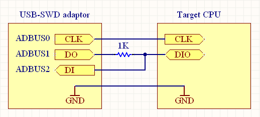

A similar scheme is mentioned in the OpenOCD documentation, but they suggest a value of 470 ohms. I’ve gone with 1K because at its lowest drive setting, FTDI chips such as the FT232H only source 4 mA, and I’m never keen on overloading outputs, no matter how harmless this is supposed to be – but feel free to follow the majority opinion, and go with 470 ohms.
Some people suggest that is is necessary for the FTDI adaptor and target CPU to share a common supply. Professional JTAG adaptors do this – they take a supply from the target system, and use level-shifters to ensure the signals are of the right amplitude – but it should’t be necessary providing your supplies are of reasonable quality. However, you must resist the temptation to make the cables very long; we’re dealing with fast edge-sensitive signals, so I’d keep the cable length below 6 inches (150 mm).
A convenient way of incorporating the resistor in a cable is by soldering & covering with heat-shrink tubing; at a pinch you could use a screw-terminal block, but try to keep the assembly reasonably compact to avoid EMC problems.
SWD Protocol
There are 3 main difficulties with this protocol:
- Bit-oriented rather than byte-oriented
- Bi-directional data line
- Intolerant of errors
The first of these is quite a culture-shock; when dealing with bit values, they are usually aggregated up to the nearest byte or word. This isn’t good enough for SWD; if you are supposed to be sending 2 bits, it must be 2 bits, not padded out to the nearest byte.
The second issue makes debugging the software quite challenging; if there is a bug that causes both sides to transmit at the same time, it is difficult to work out which side is at fault.
The third issue is actually a design feature; in the event of an error, the CPU interface is designed to stop transmitting, to avoid further data collisions – but when writing your own code, you often find the target CPU stops talking; it refuses to communicate, and you don’t know why.
To give an example, here is the standard SWD read transaction on which all data transfers are based, taken from the original ARM document “Serial Wire Debug and the CoreSight Debug and Trace Architecture”. All transactions are initiated and controlled by the SWD adaptor, the target CPU just ‘fills in the blanks’ in the messages it is given.

We start with the data line being idle, which (very confusingly) can be either high or low. The clock line can be either be running continuously, or can stop between transactions; a bit like Ethernet, in that the recipient looks for a specific marker in the data, and ignores everything until that is received. In this context, the marker is at least 2 low (zero) bits, followed by a high ‘start’ bit, then there are 7 bits of header data. If you want to know the meaning of these bits, ARM have copious online documentation, such as the “CoreSight Components Technical Reference Manual”.
After the initial transmission to the CPU, the adaptor inserts a dummy ‘turnaround’ bit where it stops driving the data line, letting the target CPU take over. The adaptor continues toggling the clock line while the CPU sends 3 acknowledgement bits; if these show a positive response (100, l.s.bit first, so a value of 1) then 32 bits of data will follow, and a parity bit. This concludes the transaction, but another turnaround bit is needed so the SWD adaptor can start driving the bus again.
Alternatively, the acknowledgement bits may show an error (001, which is a value of 4), in which case the CPU will stop communicating, or a ‘wait’ indication (010, a value of 2), which means the data isn’t yet available – try again later.
After this transaction, another may follow immediately, or a minimum of 2 zero bits may be inserted to idle the data line – a clean transition between transactions is essential, with no spurious additional bits.
Python implementation
After several false starts, I ended up creating my own class to store bit values; there are various bit-handling libraries around, but my requirements are so simple that these are massive overkill.
# Class for a multi-bit value
class Bitval(object):
    def __init__(self, value, nbits, name="", rd=False):
        self.value = value
        self.nbits = nbits
        self.name = name
        self.rd = rd
That’s all – it is just a vehicle for storing one or more bits; the ‘name’ isn’t strictly necessary, but is useful in identifying one bit-value amongst many others.
The ‘rd’ flag indicates whether the value should be write-only, or whether we need the value to be read back from the target system. For example, in the SWD read cycle above, we need to know the ‘ack’ and ‘data’ values, but aren’t really interested in reading back the other bits we’re sending – and the FTDI device provides a convenient way of controlling whether input data is read back or not (command bit 5: ‘TDO/DI data input’).
Creating the SWD request is just a question of stacking the bit-values in a list, e.g.
# 1 start bit, 1 AP bit, 1 read bit, 2 address bits...
Bitval(1, 1, "Start"),      Bitval(ap,   1, "AP"),
Bitval(1, 1, "Read"),       Bitval(addr, 2, "Addr"), etc..
Our USB driver software just churns out the bit-values in sequence, then gets any responses that are required; it doesn’t need to understand what each bit-value means. All that is needed is a bit of support code, to allow iteration through the list, and give access to the important element values:
# Create an SWD read request for a given AP or DP address
class swd_rd_request(object):
    def __init__(self, ap, addr):
        addr >>= 2
        hpar = ap ^ 1 ^ (addr & 1) ^ (addr>>1 & 1)
        self.ack = Bitval(0, 3, "Ack", 1)
        self.data = Bitval(0, 32, "Data", 1)
        self.dparity = Bitval(0, 1, "DParity", 1)
        self.bitvals = (
            Bitval(1, 1, "Start"),      Bitval(ap, 1, "AP"),
            Bitval(1, 1, "Read"),       Bitval(addr, 2, "Addr"),
            Bitval(hpar, 1, "HParity"), Bitval(0, 1, "Stop"),
            Bitval(1, 1, "Park"),       Bitval(0, 1, "Turn"),
            self.ack,                   self.data,
            self.dparity,               Bitval(0, 1, "Turn"))

    # Allow the bitval list to be iterated
    def __getitem__(self, idx):
        bv = self.bitvals[idx]
        return bv
Having set up a class for our data transaction, it is easy to transmit the data, and evaluate the response:
req = swd_rd_request(ap, addr)  # Create request
for bv in req:                  # For each bit-value..
    spi_write_bitval(h, bv)     # ..send bit(s) out
for bv in req:                  # For each bit-value..
    if bv.rd:                   # .. with 'rd' flag set..
        spi_read_bitval(h, bv)  # .. read bit(s) in
Since the request is a class instance, we can access the returned bits in an intuitive way, e.g. simplistically:
if req.ack.value == 1:     # If request was acknowledged OK..
    print(req.data.value)  # ..print returned data value
SWD reset
Now that we have an easy way to send an SWD request, can we read something out from the CPU? Nearly, there is just the reset process to go through.
To unlock the CPU SWD interface and start communicating, we need to send a lengthy bit sequence, namely at least 50 ‘1’ bits, then 0111 1001 1110 0111 (9E E7 hex, l.s.bit first), then at least another 50 ‘1’ bits, then at least 2 ‘0’ bits. this serves 2 purposes:
- It provides a unique bit-pattern, that can’t be confused with a normal request
- It gives time for the CPU SWD interface to be powered up
The second point is important; ARM CPUs are designed with power-saving in mind, and parts of the CPU may be powered down when not in use, so need some time to wake up. This especially applies if the CPU is in a deep sleep mode; it may require the startup sequence to be sent several times before the CPU is sufficiently awake to respond to requests. Despite the ‘reset’ name, this sequence does not reset the error-handling of the SWD interface; that must be done using a separate write-cycle.
Reading the CPU ID
After sending the startup sequence, the first request should be a read of the CPU ID; not just because it is a simple read-only value, but also because the CPU specification may require that it be read before anything else.
We need to set the ‘ap’ and ‘addr’ values in the code above; I’ll describe these settings in detail in the next post, but for now, it is sufficient to say that the ID register is at DP address 0, so ap=0, addr = 0.
So we just need to send the startup bit pattern, then a request with these values, and read back the result. If we’re unlucky, it’ll be all-0s because the target CPU isn’t communicating, or all-1s because the data line is floating; ideally it is something between those, that is consistent every time it is read; on an STMicro Cortex M3 CPU (STM32F103) it is 1BA01477, see your CPU’s data sheet for the corresponding value.
See below for the full Python source code to read the ID register; I can’t claim this code is particularly useful on its own, but in the next post we’ll start to explore some more useful data requests.
Regrettably the code doesn’t work on Linux with libftdi. In all my tests the SPI write cycles work fine, but the read cycles always return null data. To be investigated.
# Python FTDI SWD example from iosoft.blog
# Compatible with Python 2.7 or 3.x
#
# v0.01 JPB 8/12/18

import time, ftdi_py_part3 as ft

VERBOSE  = False    # Flag to display SWD read/write cycles
ERRVAL = 0xEEEEEEEE # Dummy value returned if read cycle fails

SWD_DP          = 0     # AP/DP flag bits
SWD_AP          = 1
DPORT_IDCODE    = 0x0   # ID Code address

SWD_ACK_OK      = 1     # SWD Ack values
SWD_ACK_WAIT    = 2
SWD_ACK_ERROR   = 4

FTDI_MODE_BITBANG   = 1     # MPSSE modes
FTDI_MODE_MPSSE     = 2

FTDI_SPI_WR_CLK_NEG = 0x01  # SPI command bit values
FTDI_SPI_BIT_MODE   = 0x02
FTDI_SPI_RD_CLK_NEG = 0x04
FTDI_SPI_LSB_FIRST  = 0x08
FTDI_SPI_WR_TDI     = 0x10
FTDI_SPI_RD_TDO     = 0x20
FTDI_SPI_WR_TMS     = 0x40

# Commands to read, write, and read+write SPI data
SPI_WR_BYTES    = FTDI_SPI_WR_CLK_NEG|FTDI_SPI_LSB_FIRST|FTDI_SPI_WR_TDI
SPI_RD_BYTES    = FTDI_SPI_LSB_FIRST|FTDI_SPI_RD_TDO
SPI_RD_WR_BYTES = SPI_RD_BYTES|SPI_WR_BYTES
SPI_RD_BITS     = SPI_RD_BYTES|FTDI_SPI_BIT_MODE
SPI_WR_BITS     = SPI_WR_BYTES|FTDI_SPI_BIT_MODE
SPI_RD_WR_BITS  = SPI_RD_BITS|SPI_WR_BITS

# Class for a bit value (1 - 32 bits)
class Bitval(object):
    def __init__(self, value, nbits, name="", rd=False):
        self.value = value
        self.nbits = nbits
        self.name = name
        self.rd = rd

# Send SWD reset; at least 50 high bits around 0111 1001 1110 0111
# (9E E7 lsb-first), then at least 2 null bits before start bit
def swd_reset(d):
    rst = (0xFF,0xFF,0xFF,0xFF,0xFF,0xFF,0xFF, 0x9E,0xE7,
           0xFF,0xFF,0xFF,0xFF,0xFF,0xFF,0xFF)
    spi_write_bytes(d, SPI_WR_BYTES, rst)
    spi_write_bits(d, SPI_WR_BITS, 0, 4)

# Send a number of idle (zero) bytes
def swd_idle_bytes(d, n):
    data = n * [0]
    spi_write_bytes(d, SPI_WR_BYTES, data)

# Create an SWD read request for a given AP or DP address
class swd_rd_request(object):
    def __init__(self, ap, addr):
        addr >>= 2
        hpar = ap ^ 1 ^ (addr & 1) ^ (addr>>1 & 1)
        self.ack = Bitval(0, 3, "Ack", 1)
        self.data = Bitval(0, 32, "Data", 1)
        self.dparity = Bitval(0, 1, "DParity", 1)
        self.bitvals = (
            Bitval(1,    1, "Start"),  Bitval(ap,   1, "AP"),
            Bitval(1, 1, "Read"),      Bitval(addr, 2, "Addr"),
            Bitval(hpar, 1, "HParity"),Bitval(0, 1, "Stop"),
            Bitval(1,    1, "Park"),   Bitval(0,    1, "Turn"),
            self.ack,                  self.data,
            self.dparity,              Bitval(0, 1, "Turn"))

    # Allow the bitval list to be iterated
    def __getitem__(self, idx):
        bv = self.bitvals[idx]
        return bv

# Create an SWD write request for a given AP or DP address
class swd_wr_request(object):
    def __init__(self, ap, addr, value):
        addr >>= 2
        hpar = ap ^ (addr & 1) ^ (addr>>1 & 1)
        self.ack = Bitval(0, 3, "Ack", 1)
        self.data = Bitval(value, 32, "Data")
        self.dparity = Bitval(parity32(value), 1, "DParity")
        self.bitvals = (
            Bitval(1,    1, "Start"),  Bitval(ap,   1, "AP"),
            Bitval(0, 1, "Read"),      Bitval(addr, 2, "Addr"),
            Bitval(hpar, 1, "HParity"),Bitval(0, 1, "Stop"),
            Bitval(1,    1, "Park"),   Bitval(0,    1, "Turn"),
            self.ack,                  Bitval(0,    1, "Turn"),
            self.data,                 self.dparity)

    # Allow the bitval list to be iterated
    def __getitem__(self, idx):
        bv = self.bitvals[idx]
        return bv

# Send an SWD read request and/or get the response
def swd_rd(d, ap, addr, tx=True, rx=True):
    req = swd_rd_request(ap, addr)
    ok = False
    if tx:
        spi_write_bitvals(d, req)
        ok = True
    if rx:
        ok = spi_read_bitvals(d, req)
    if VERBOSE:
        if rx:
            print("  Rd %X %-7s %08lX Ack %u" % (addr,
                  apreg_str(addr) if ap else dpreg_str(addr, 1),
                  req.data.value, req.ack.value))
        else:
            print("  Rd %X %-7s" % (addr,
                  apreg_str(addr) if ap else dpreg_str(addr, 1)))
    return req if ok else None

# Send an SWD write request and/or get the response
def swd_wr(d, ap, addr, value, tx=True, rx=True):
    req = swd_wr_request(ap, addr, value)
    ok = False
    if tx:
        spi_write_bitvals(d, req)
        ok = True
    if rx:
        ok = spi_read_bitvals(d, req)
    if VERBOSE:
        if rx:
            print("  Wr %X %-7s %08lX Ack %u" % (addr,
                  apreg_str(addr) if ap else dpreg_str(addr, 0),
                  req.data.value, req.ack.value))
        else:
            print("  Wr %X %-7s %08lX" % (addr,
                  apreg_str(addr) if ap else dpreg_str(addr, 0),
                  req.data.value))
    return req if ok else None

# Return DP register string
def dpreg_str(reg, rd):
    if rd:
        s = ("IDCODE" if reg==0 else "STATUS" if reg==4 else
             "RESEND" if reg==8 else "RDBUFF")
    else:
        s = ("ABORT " if reg==0 else "CTRL" if reg==4 else
             "SELECT" if reg==8 else "RDBUFF")
    return s

# Return AP register string; see Cortex-M3 'AHB-AP programmers model'
def apreg_str(reg):
    return ("CSW/BD0" if reg==0 else "TAR/BD1" if reg==4 else
            "BD2/RAR" if reg==8 else "DRW/BD3")

# Write bitval requests
def spi_write_bitvals(d, bitvals):
    for bv in bitvals:
        spi_write_bitval(d, bv)

# Read bitval responses
def spi_read_bitvals(d, bitvals):
    ok = True
    for bv in bitvals:
        ok = spi_read_bitval(d, bv)
        if not ok:
            break
    return ok

# Write a bit value to SPI interface
# If read-flag is set, use read+write, otherwise just write
def spi_write_bitval(d, bv):
    value, nbits = bv.value, bv.nbits
    cmd = SPI_RD_WR_BITS if bv.rd else SPI_WR_BITS
    while nbits > 0:
        n = min(nbits, 8)
        spi_write_bits(d, cmd, value&0xff, n)
        value >>= n
        nbits -= n

# Read a bit value (max 32 bits) from SPI, if read-flag is set
def spi_read_bitval(d, bv):
    ok = True
    if bv.rd:
        bv.value = shift = 0
        nbits = bv.nbits
        while ok and nbits >= 8:    # Get whole bytes
            data = spi_read_bytes(d, 1)
            if len(data) > 0:
                byt = data[0] >> max(8-nbits, 0)
                bv.value |= byt  0:
                bv.value = data[0]
            else:
                bv.value = ERRVAL
                ok = False
    return ok

# Write SPI command and data bytes to the device
def spi_write_bytes(d, cmd, data):
    n = len(data) - 1
    ft.ft_write(d, [cmd, n&0xff, n>>8] + list(data))

# Read data bytes back from SPI
def spi_read_bytes(d, nbytes):
    return ft.ft_read(d, nbytes)

# Write SPI command and up to 8 bits to the device
def spi_write_bits(d, cmd, byt, nbits):
    ft.ft_write(d, (cmd, nbits-1, byt))

# Read data bits back from SPI
# Bits are left-justified in the byte, so must be shifted down
def spi_read_bits(d, nbits):
    data = ft.ft_read(d, 1)
    return [data[0] >> (8-nbits)] if len(data)>0 else []

# Calculate parity of 32-bit integer
def parity32(i):
    i = i - ((i >> 1) & 0x55555555)
    i = (i & 0x33333333) + ((i >> 2) & 0x33333333)
    i = (((i + (i >> 4)) & 0x0F0F0F0F) * 0x01010101) >> 24
    return i & 1

if __name__ == "__main__":
    dev = ft.ft_open()
    if not dev:
        print("Can't open FTDI device")
    else:
        ft.set_bitmode(dev, 0, 2)           # Enable SPI
        ft.set_spi_clock(dev, 1000000)      # Set SPI clock
        ft.ft_write(dev, (0x80, 0, ft.OPS)) # Set outputs
        swd_reset(dev)                      # Send SWD reset sequence
        r = swd_rd(dev, SWD_DP, DPORT_IDCODE) # Request & response
        if r is None:
            print("No response")
        else:
            print("SWD ack %u, ID %08Xh" % (r.ack.value, r.data.value))
        dev.close()
# EOF
In the next post we’ll be doing something a bit more useful – accessing the CPU address space.
Copyright (c) Jeremy P Bentham 2018. Please credit this blog if you use the information or software in it.

One thought on “Programming FTDI devices in Python: Part 4”