
Hardware
I’m starting this project with the Raspberry Pi ZeroW, which uses the Cypress WiFi chip CYW43438. It interfaces to the ARM processor using Secure Digital I/O (SDIO), which consists of the following signals:
- Clock (1 line, O/P from CPU)
- Command (1 line, I/O)
- Data (4 lines, I/O)
Later in this blog, I’ll be describing what these pins do, in case you are a newcomer to the strange world of SDIO.
The I/O bit numbers are defined in the DeviceTree file for the board:
sdio_pins {
    brcm,pins = <0x00000022 0x00000023 0x00000024 0x00000025 0x00000026 0x00000027>;
    brcm,function = <0x00000007>;
    brcm,pull = <0x00000000 0x00000002 0x00000002 0x00000002 0x00000002 0x00000002>;
    phandle = <0x00000019>;
};
The ‘pull’ settings show that pullup resistors are enabled for pin 23 to 27 hex (GPIO35 to 39), and an initial guess would be that these pins are the command and data, while 22 hex (GPIO34) is the clock.
The datasheet mentions a power-on signal, and a quick trawl on the Web suggests that this could be GPIO41, which must be high to power up the WiFi interface. There is also mention of a low-speed (32 kHz) clock that may be needed when waking up the chip from low-power mode; it turns out this is on GPIO43. This can be verified by dumping the I/O configuration registers when the WiFi interface is running:
  20300000: 0013D660 00017030 A5040030 353A0002 00001000 00000000 00000000 00000000
  20300020: 00000000 01FF0000 00000F02 000E0207 00000000 00FF0133 00FF0133 00000000
Each pin has a 3-bit mode value, that shows whether it being used for simple input, output, or is connected to an internal peripheral (ALT0 – 5). The values above can be decoded by referring to the ‘BCM2835 ARM Peripherals’ data sheet, but an easier way is to use the ‘pigs’ front-end for the PIGPIO library, thus:
sudo pigpiod   [load PIGPIO daemon]
pigs mg 34     [get mode of GPIO pin 34]
7              [returned value 7: pin is ALT3]
pigs mg 43     [get mode of GPIO pin 43]
4              [returned value 4: pin is ALT0]
Pins 34 to 39 are all set to ALT3, which is unhelpfully labelled in the BCM2835 datasheet as ‘reserved’; in reality this means they are connected to the (undocumented) Arasan SD controller. GPIO43 is configured as ALT0, which is the clock source GPCLK2, configured for 32.768 kHz.
Attaching a logic analyser
To understand what the Linux driver is doing, I need to attach a logic analyser to the SDIO bus. This isn’t easy on most boards; the interface runs very fast (up to 50 MHz) so the only means of attachment is by soldering onto extremely small surface-mount components, that can easily be damaged.
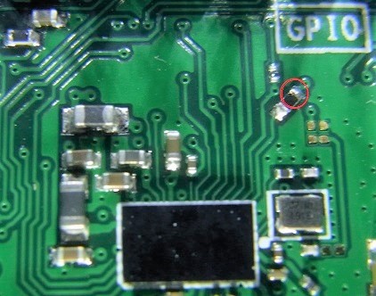
However, the Pi Zerow has some interesting pads on the underside.
Those 7 gold circles are clearly attached to some internal signals, since they have conductive holes (known as ‘vias’) to tracks on other layers. Also, they’re in the right area for the SDIO interface, and it is possible they’re needed for testing the WiFi/ Bluetooth interface after the PCB is assembled. Monitoring these signals with WiFi running proved that they do have almost all of the SDIO signals, aside from the most important one: the clock. Further probing suggested that the only way to pick up that signal is on the other side of the board at a resistor, but connecting to this point is tricky; you need good surface-mount soldering skills to avoid damaging the board.
The main problem with the logic analyser interface is the sheer volume of data that’ll be accumulated. The boot process takes around a minute, with sporadic activity on the SDIO interface; catching all that, with a data rate of 50 MHz, would require a very complicated and/or expensive setup. Fortunately, the Raspberry Pi has an ‘overclocking’ setting in the boot file config.txt, which sets the clock rate to be used when the OS requests 50 MHz. This doesn’t just speed up the interface; a value of 1 or 2 MHz can be used to slow it right down, e.g.
# Add to /boot/config.txt:
dtparam=sdio_overclock=2
This allows a lower-cost analyser to be used (see part 1 of this blog for details) – and surprisingly, the change doesn’t make a lot of difference to the boot-time, since there are long pauses in SDIO activity, where the OS is doing other things. This can be seen by zooming the analyser display out to the maximum, showing 50 seconds of data:
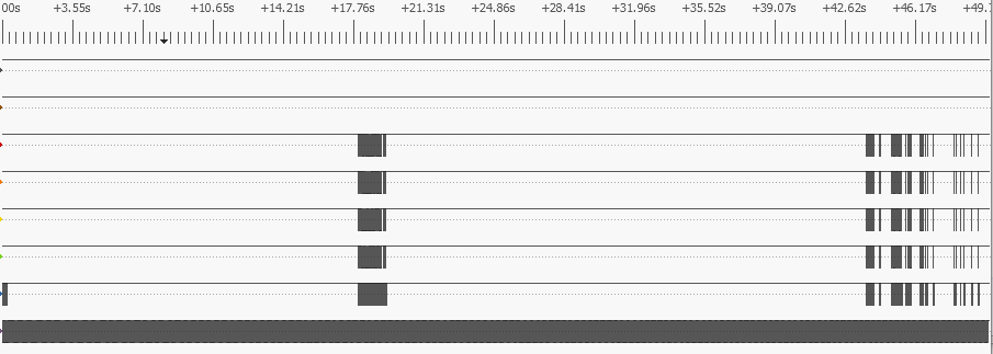
The bottom trace is the clock, the next is the command (CMD) line, then there are the 4 data lines. Despite the long periods with no activity, there is a lot going on: over 2,200 commands and 13,000 data blocks are being exchanged between the CPU and the WiFi chip.
SDIO protocol
If, like me, you have some experience of the Serial Peripheral Interface (SPI), you may expect SDIO to be similar, in that it uses a clock line to synchronise the sender & receiver; the rising edge of the clock indicates that the data is stable, and can be read by the receiver.
However, there are a few key differences:
- Bi-directional. All the lines, apart from the clock, are bi-directional; either side can drive them.
- Command and data lines. There are separate lines for commands and data, and the 4 data lines act as a 4-bit parallel bus.
- Start & end bits. Instead of the SPI chip-select, the data and command lines idle high, then go low to signal the start of a transfer; this is referred to as a ‘start bit’, and is a single bit-time with a value of zero. At the end of the transfer there is a single bit with a value of 1, an ‘end bit’.
- Format. The format of SDIO commands and responses is standardised, with specific meaning to the transferred bytes.
It is well worth reading the SDIO specification; at the time of writing, the latest version that is available from the SD Association is “SD Specifications Part E1, SDIO Simplified Specification Version 3.00”. For a few of the commands you need to refer back to the “SD Specifications Part 1 Physical Layer Simplified Specification”, for example:
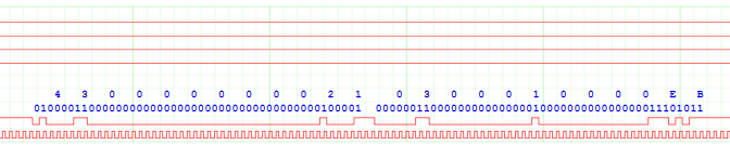
This is SD command 3 (generally abbreviated to CMD3) and response 6 (R6) from the target (WiFi chip). Both are specified at being 48 bits long, and you can see they begin with a 0 start-bit, and finish with a 1 end-bit. Between the two, the command line is briefly idle. It is a bit confusing that the reply to a command 3 is not a response 3; this is because there are a lot of commands (over 50) but many of them share the same response format, so only 7 possible responses have been defined.
The most common commands used in the SDIO interface are CMD52 and 53. Command 52 is used to read or write a single 8-bit value, while CMD53 transfers blocks of data, either singly or in batches. The following trace shows command 53 reading a single block of 4 data bytes; the command and response look similar to command 52, but there is also activity on the data lines, starting with a 4-bit value of zero, and ending with F hex.

SDIO interface code
In the absence of the necessary documentation, writing code for the ‘Arasan’ SD controller on the Raspberry Pi would be quite fraught, so I decided to use direct control (‘bit-bashing’ or ‘bit-banging’) of the I/O lines. The more experienced among you might be thinking this is a really bad idea, as it can be very CPU-intensive and slow, but I believe that the end-result (for example, booting the WiFi chip from scratch in 1 second) vindicates my decision – and if you want to use the controller, you can modify my code to do so.
The bit-patterns within the SDIO commands and responses are quite complex, and the code I’ve seen makes heavy use of bit-masking and shifting to combine the individual values into a single message. I’m not a fan of this approach, and prefer to use C language bitfields. For example, CMD52 has the following fields in the 6-byte message:
Start:             1 bit  (always 0)
Direction:         1 bit  (1 for command, 0 for response)
Command index:     6 bits (52 decimal for command 52)
R/W flag:          1 bit  (0 for read, 1 for write)
Function number:   3 bits (select the bus, backplane or radio interface)
RAW flag:          1 bit  (1 to read back result of write)
Unused:            1 bit
Register address: 17 bits (128K address space)
Unused:            1 bit
Data value:        8 bits (byte to be written, unused if read cycle)
CRC:               7 bits (cyclic redundancy check)
End:               1 bit  (always 1)
You’ll see that the values don’t all line up on convenient 8-bit boundaries; furthermore the data sheet defines the values with most-significant value first, whereas standard C structures have least-significant first.
My solution is to use macros to reverse the order of bits in the byte, so the command structure looks similar to the specification. These are used to create structures for the commands and responses, which are combined in a union.
#define BITF1(typ, a)             typ a
#define BITF2(typ, a, b)          typ b, a
#define BITF3(typ, a, b, c)       typ c, b, a
..and so on..

typedef struct
{
    BITF3(uint8_t,  start:1, cmd:1,   num:6);
    BITF5(uint8_t,  wr:1,    func:3,  raw:1, x1:1, addrh:2);
    BITF1(uint8_t,  addrm);
    BITF2(uint8_t,  addrl:7, x2:1);
    BITF1(uint8_t,  data);
    BITF2(uint8_t,  crc:7,   stop:1);
} SDIO_CMD52_STRUCT;

typedef union
{
    SDIO_CMD52_STRUCT   cmd52;
    SDIO_RSP52_STRUCT   rsp52;
    SDIO_CMD53_STRUCT   cmd53;
    uint8_t             data[MSG_BYTES+2];
} SDIO_MSG;
The code to split the 17-bit address into 3 bytes is still a bit messy, but the structure definition does simplify the process of creating a command:
// Send SDIO command 52, get response, return 0 if none
int sdio_cmd52(int func, int addr, uint8_t data, int wr, int raw, SDIO_MSG *rsp)
{
    SDIO_MSG cmd={.cmd52 = {.start=0, .cmd=1, .num=52,
        .wr=wr, .func=func, .raw=raw, .x1=0, .addrh=(uint8_t)(addr>>15 & 3),
        .addrm=(uint8_t)(addr>>7 & 0xff), .addrl=(uint8_t)(addr&0x7f), .x2=0,
        .data=data, .crc=0, .stop=1}};

    return(sdio_cmd_rsp(&cmd, rsp));
}
For speed, the CRC is created using a byte-wide lookup table in RAM, which is computed on startup:
#define CRC7_POLY    (uint8_t)(0b10001001 << 1)

uint8_t crc7_table[256];

// Initialise CRC7 calculator
void crc7_init(void)
{
    for (int i=0; i<256; i++)
        crc7_table[i] = crc7_byte(i);
}

// Calculate 7-bit CRC of byte, return as bits 1-7
uint8_t crc7_byte(uint8_t b)
{
    uint16_t n, w=b;

    for (n=0; n<8; n++)
    {
        w <<= 1;
        if (w & 0x100)
            w ^= CRC7_POLY;
    }
    return((uint8_t)w);
}

// Calculate 7-bit CRC of data bytes, with l.s.bit as stop bit
uint8_t crc7_data(uint8_t *data, int n)
{
    uint8_t crc=0;

    while (n--)
        crc = crc7_table[crc ^ *data++];
    return(crc | 1);
}
Data CRC
The data transfer includes a CRC for every line, for example this is the transfer of the 4 bytes A6, A9, 41, and 15 hex.
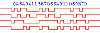
A total of 12 bytes are transferred, because each data line has an added 16-bit CRC. This was a bit of a headache, since splitting the 4-bit data into individual 1-bit values for CRC calculation would considerably slow down the command generation & checking. Fortunately there is a easy way to calculate & check the CRC for each line, while still keeping the 4 values together. This comes from the realisation that the exclusive-or operation in the CRC doesn’t care what order the bits are in; we can rearrange the bits to match our data. So we can compute all 4 CRCs using a single 64-bit value:
Bit 0: bit 0 of 1st CRC
Bit 1: bit 0 of 2nd CRC
Bit 2: bit 0 of 3rd CRC
Bit 3: bit 0 of 4th CRC
Bit 4: bit 1 of 1st CRC
..and so on, up to..
Bit 63: bit 15 of 4th CRC
Once they have been computed, the 4 CRCs are transmitted by just shifting out the next 4 bits of the 64-bit value. To speed up the calculation, a 4-bit lookup table is initialised on startup:
#define CRC16R_POLY  (1<<(15-0) | 1<<(15-5) | 1<<(15-12))

uint64_t qcrc16r_poly, qcrc16r_table[16];

// Initialise bit-reversed CRC16 lookup table for 4-bit values
void qcrc16r_init(void)
{
    qcrc16r_poly = quadval(CRC16R_POLY);
    for (int i=0; i<(1<<SD_DATA_PINS); i++)
        qcrc16r_table[i]  = (i & 8 ? qcrc16r_poly<<3 : 0) |
                            (i & 4 ? qcrc16r_poly<<2 : 0) |
                            (i & 2 ? qcrc16r_poly<<1 : 0) |
                            (i & 1 ? qcrc16r_poly<<0 : 0);
}

// Spread a 16-bit value to occupy 64 bits
uint64_t quadval(uint16_t val)
{
    uint64_t ret=0;

    for (int i=0; i<16; i++)
        ret |= val & (1<<i) ? 1LL<<(i*4) : 0;
    return(ret);
}
Now when transmitting, the 64-bit (i.e. 4 x 16-bit) CRC is updated with every 4-bit value:
uint64_t qcrc=0;

// For each 4-bit value 'd':
qcrc = (qcrc >> 4) ^ qcrc16r_table[(d ^ (uint8_t)qcrc) & 0xf];
After the data has been sent, the CRC values are transmitted:
for (n=0; n<16; n++)
{
    output((uint8_t)qcrc & 0xf);
    qcrc >>= 4;
}
Bulk transfers
Command 53 can be used to transfer a single block (where the block size is specified in the command) or multiple blocks (where the block size has previously been set, and the number of blocks is specified in the command).
If the CPU is sending a single command, then writing multiple blocks to the WiFi chip, how does it check that the blocks are being received and processed OK? The answer is that when writing blocks, the recipient generates a brief acknowledgement back. Here is an example of a CMD53 write.

It is a bit difficult to see what is going on; the command and response are similar to all the others, but then (after a surprisingly long pause) the data is transferred from the CPU to the WiFi chip. Zooming in on that data:

4 bytes with the values 3, 0, 0, 0, are being transferred, then 8 bytes of CRC. However, after that, the recipient acknowledges the received data by driving the least-significant data line with a bit value of 00101000 00111111 (28 3F hex). To be honest, I haven’t been able to find a proper description of these bits; I assume there is a single byte value, then the recipient holds the line low until it has finished processing, but the meaning of the byte bits isn’t at all clear. So for the time being, my code reads in the byte value, then waits for the line to go high, effectively treating it as a ‘busy bit’.
Clock polarity
A small but significant detail is the relationship between the data changes and the clock edges – when is the data stable so it can be read? I previously suggested that the data is read on the positive clock-edge, but look at this trace showing the transition between the command and the response:

For the command, the data changes on the negative-going clock edge, so can be read on the positive-going edge. The response appears to be the opposite way around, with the data changing on the positive-going edge – what is going on?
The answer is that the WiFi chip has been set to ‘SDIO High-Speed’ mode; the data changes very shortly after the positive-going edge of the clock, so as to enable fast transfers. The timing is described in the chip data sheet if you want to know the details, but the end result is that the logic analyser isn’t fast enough to capture the gap between clock & data changes, so the software that analyses the logic traces has to use the last state before the clock goes high.
Bit bashing
The bit-bash (or bit-bang) code was quite difficult to write; it has to toggle the clock line, feed out the single-bit command, then get the response whilst simultaneously sending or receiving the 4-bit data. Also, although the examples above show the data being shorter than the response, in reality it can be considerably longer, up to 512 bytes, so will finish long after the activity on the command line. Then there is the issue of the acknowledgements of block data writes, and the need for a timeout in case the chip goes unresponsive…
There is no point describing the code here; if you are interested, take a look at the source. In theory, it’d be a good idea to replace it with a driver for the Arasan SD controller, but I’m not sure there would be a large speed gain – the Linux driver seems to spend a lot of time idle, waiting for the SD controller to complete a task. Also the bit-bashing code is more universal: it shouldn’t be too difficult to port it to other processors such as the STM32, which is frequently paired with the Cypress chip in a standalone module.
SPI interface
For completeness, I need to mention that according to the data sheet, the WiFi chip has a Serial Peripheral Interface (SPI), that can be used instead of SDIO. This is enabled by sending a reset command to the chip, while certain I/O lines are held in specific states.
I originally thought this interface would be easier to use than SDIO, but all my attempts to get it working failed. Also, the SPI connections don’t seem to line up with the SPI master in the BCM2835, so the interface would have to be bit-bashed, which would be really slow as the data bus is only 1-bit-wide. So I abandoned SPI, and focused exclusively on SDIO.
[Overview] [Previous part] [Next part]
Copyright (c) Jeremy P Bentham 2020. Please credit this blog if you use the information or software in it.
