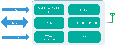
This diagram shows the internals of the CYW43xxx chip in simplified form; the important point is that the chip has its own CPU, RAM and ROM; it is a computer-within-a-computer.
In part 2 I mentioned the lack of documentation, and now this becomes a major issue; how to program this complex chip, with no data on its internals. Cypress have partially solved this problem by issuing a standard binary ‘blob’ (roughly 300K bytes) that contains all the code for the embedded CPU; we’ll just be feeding data and control messages into that program, not knowing (or caring) what it is doing to the chip hardware.
I say the problem is ‘partially’ solved because we have to set up the chip to receive this program, upload the code into its RAM, then configure the chip to run it.. a sizeable task, as I’ve discovered.
First steps
The first task is to get the WiFi chip to respond to our commands. The SD and SDIO specifications offer plenty of flowcharts that describe how such a device might be initialised, but I had minimal success with these; they may be applicable to older chips, but maybe the later incarnations of the CYW43xxx just treat the SDIO bus as a convenient parallel interface, rather than slavishly following a specification that was designed for plug-in SD cards.
Then there are the timing issues; a quick glance at the existing code shows many instances where SDIO commands are artificially delayed; after you change something within the chip, it needs time to react before receiving the next command – and if that is sent too quickly, the chip just ignores it, with no error response.
The best way I could find to tackle these problems is to capture all the SDIO commands, responses & data when the Linux driver is running. The capture method is described in the previous part of this blog, and it results in a sizeable file: over 5 gigabytes as a CSV. It contains over 2,200 commands and 13,000 data blocks, so I wrote an application (‘sd_decoder’) to decode the file and display the commands. It turns out that there is a lot of redundancy (for example, the driver loads the 300K binary into the chip, then reads it all back again) so by focusing purely on one WiFi chip, we can make major simplifications.
Fragments of the simplified command sequence can then be replayed into the chip, and eventually, it starts to respond – the first time you get a response from a new chip is a happy day! Here are the first few commands the Linux driver uses to start up the chip:
 0.000331 74 00 00 0c 00 39 * Cmd 52 00000C00 Rd BUS  00006
 0.002759 74 80 00 0c 08 9f * Cmd 52 80000C08 Wr BUS  00006 08
 0.025217 40 00 00 00 00 95 * Cmd  0 00000000
 0.028130 48 00 00 01 aa 87 * Cmd  8 000001AA
 0.028527 45 00 00 00 00 5b * Cmd  5 00000000
 0.028660 3f 20 ff ff 00 ff ? Rsp 63 20FFFF00
 0.028875 45 00 20 00 00 3d * Cmd  5 00200000
 0.029007 3f a0 ff ff 00 ff ? Rsp 63 A0FFFF00
 0.029228 43 00 00 00 00 21 * Cmd  3 00000000
 0.029353 03 00 01 00 00 eb * Rsp  3 00010000
 0.029690 47 00 01 00 00 dd * Cmd  7 00010000
 0.029815 07 00 00 1e 00 a1 * Rsp  7 00001E00
To explain the format; firstly the time in seconds, then 6 command/response bytes, ‘*’ to indicate CRC is correct, or ‘?’ if incorrect, then a partial decode.
A few points to note:
- The first 4 commands produce no responses.
- There are jumps in the timestamp, presumably caused by intentional delays.
- CMD5 is described in the SDIO specification as enabling I/O mode, but the response we get has an incorrect CRC.
- The CMD3 – CMD7 sequence is described in the SD specification; it is the way that a host selects one card from multiple card slots; CMD3 gets a Relative Card Address (RCA), then command 7 selects the card using that address.
It’d be nice to understand why two of the commands have failed CRCs, but the Linux driver ignores that error, so I will as well. The above sequence is implemented in my code as follows:
int rca;
sdio_cmd52(SD_FUNC_BUS, 0x06, 0, SD_RD, 0, 0);
usdelay(20000);
sdio_cmd52(SD_FUNC_BUS, 0x06, 8, SD_WR, 0, 0);
usdelay(20000);
sdio_cmd(0, 0, 0);
sdio_cmd(8, 0x1aa, 0);
// Enable I/O mode
sdio_cmd(5, 0, 0);
sdio_cmd(5, 0x200000, 0);
// Assert SD device
sdio_cmd(3, 0, &resp);
rca = SWAP16(resp.rsp3.rcax);
sdio_cmd7(rca, 0);
Note the time delays; it is tempting to reduce them, but I have found from bitter experience that this can result in major problems much later on (as a critical setting has been ignored), so I wouldn’t recommend doing that.
Raspberry Pi I/O
Now it is necessary to translate the SDIO commands into hardware I/O cycles. The good news about bare-metal programming is that is isn’t necessary to use a fancy driver, or seek permission from the operating system; we can just control the I/O directly.
The primary source of information is the ‘BCM2835 ARM Peripherals’ document; armed with that and knowledge of the I/O base address (0x20000000 for the Pi ZeroW) we can create suitable low-level functions.
// Addresses
#define REG_BASE    0x20000000      // Pi Zero (0x3F000000 for Pi 3)
#define GPIO_BASE       (REG_BASE + 0x200000)
#define GPIO_MODE0      (uint32_t *)GPIO_BASE
#define GPIO_SET0       (uint32_t *)(GPIO_BASE + 0x1c)
#define GPIO_CLR0       (uint32_t *)(GPIO_BASE + 0x28)
#define GPIO_REG(a)     ((uint32_t *)a)

// Mode values
#define GPIO_IN         0
#define GPIO_OUT        1
#define GPIO_ALT0       4
#define GPIO_ALT1       5
#define GPIO_ALT2       6
#define GPIO_ALT3       7

// Configure pin as input or output
void gpio_mode(int pin, int mode)
{
    uint32_t *reg = GPIO_REG(GPIO_MODE0) + pin / 10;
    int shift = (pin % 10) * 3;

    *reg = (*reg & ~(7 << shift)) | (mode << shift);
}

// Set an O/P pin
void gpio_out(int pin, int val)
{
    uint32_t *reg = (val ? GPIO_REG(GPIO_SET0) : GPIO_REG(GPIO_CLR0)) + pin/32;

    *reg = 1 << (pin % 32);
}

// Get an I/P pin value
uint8_t gpio_in(int pin)
{
    uint32_t *reg = GPIO_REG(GPIO_LEV0) + pin/32;

    return (((*reg) >> (pin % 32)) & 1);
}
Configuring a pin as an input or output is done by setting a 3-bit values. Writing 1 or 0 to a pin is (sadly) done using separate set & clear registers; this does make any speed-optimisations (e.g. direct DMA to I/O ports) significantly harder, so I haven’t tried this yet.
Running under Linux
Although the whole purpose of this project is to run without Linux, after I’d written the above code, I did wonder whether it’d speed up development if I ran it under Linux with the WiFi interface shut down, using mmap() to gain access to the devices at low level.
This experiment failed; I never got reliable communications with the WiFi chip, and the operating system had a tendency to crash after my code was run. This isn’t too surprising, since the whole point of the OS is to control the hardware, and having a user-mode program controlling it as well, is really asking for trouble.
Timer
In addition to I/O cycles, we need a microsecond timing reference, that can be used to provide accurate delays. Fortunately there is a 32-bit register clocked at 1 MHz that is ideal for the purpose.
#define USEC_BASE       (REG_BASE + 0x3000)
#define USEC_REG()      ((uint32_t *)(USEC_BASE+4))

// Delay given number of microseconds
void usdelay(int usec)
{
    int ticks;

    ustimeout(&ticks, 0);
    while (!ustimeout(&ticks, usec)) ;
}

// Return non-zero if timeout
int ustimeout(int *tickp, int usec)
{
    int t = *USEC_REG();

    if (usec == 0 || t - *tickp >= usec)
    {
        *tickp = t;
        return (1);
    }
    return (0);
}
SDIO output
The Raspberry Pi CPU is sufficiently fast that we can easily toggle the clock line at 500 kHz, while shifting the command bits out.
#define SD_CLK_DELAY    1   // Clock on/off time in usec

// Write command to SD interface
void sdio_cmd_write(uint8_t *data, int nbits)
{
   uint8_t b, n;

    gpio_mode(SD_CMD_PIN, GPIO_OUT);
    for (n=0; n<nbits; n++)
    {
        if (n%8 == 0)
            b = *data++;
        gpio_out(SD_CMD_PIN, b & 0x80);
        b <<= 1;
        usdelay(SD_CLK_DELAY);
        gpio_out(SD_CLK_PIN, 1);
        usdelay(SD_CLK_DELAY);
        gpio_out(SD_CLK_PIN, 0);
    }
    gpio_mode(SD_CMD_PIN, GPIO_IN);
}
This code could be made much faster, by eliminating the delays. When writing the data output function I took a more aggressive approach to the timing; the transfers are error-free with a 2 MHz clock (8 Mbit/s of data) and could go faster with some optimisation.
Reception is a lot more tricky, handling command responses, data on CMD53 read-cycles, and acknowledgements on write-cycles. This requires multiple state-machines, triggered by the clock edges and ‘start’ bit detection; see the source code for details.
The 7- and 16-bit CRC calculations for commands & data have already been explained in part 2 of this blog.
[Overview] [Previous part] [Next part]
Copyright (c) Jeremy P Bentham 2020. Please credit this blog if you use the information or software in it.
