
This is the first post in a series describing a low-cost WiFi-based logic analyser, that can be used for monitoring equipment in remote or hazardous locations. For an overview of the project, see this post. The hardware specification is:
- Digital inputs: 16 for each unit
- Input threshold: programmable
- Sample rate: up to 20 megasamples per second
- Sample store: up to 250 kilosamples
- Network interface: WiFi
Wireless networking is an essential component of this project, and at the time of writing, the most logical hardware choice is the Espressif ESP32, which is a microcontroller with up to 34 GPIO pins, an Xtensa dual-core 32-bit LX6 processor, and built-in WiFi.
Sample storage
There are ESP32 variants with differing amounts RAM & flash ROM, but currently the most common type is the ESP32-S2 with 320 KiB SRAM and 128 KiB ROM. A significant portion of this is taken up by the WiFi code, so there is insufficient RAM to store the required number of samples.
When using external memory for sample storage, the standard practice is to employ one or more RAM chips and an address counter that is fed from a constant clock that increments when a sample is stored.

Unfortunately, the 16 data lines plus 18 address lines make this arrangement quite bulky, even when implemented using surface-mount parts. One way of simplifying the circuit is to embed the logic within a programmable logic device, such as a Field-Programmable Gate Array (FPGA), but the programming & debugging of such a device can be quite complex.
Ideally, what we want is a RAM device that has a built-in address counter, that will auto-increment on each sample. Such devices do exist, they are known as ‘Serial SRAM’; they have a 1-bit, 2-bit or 4-bit clocked serial interface for sending commands and data. You may be familiar with 1-bit SPI (Serial Peripheral Interface), as it is used in a wide variety of devices, and the RAM chip is in this mode on startup. Less well-known are the 2-bit (SDI or DSPI) and 4-bit (SQI or QSPI) interfaces that use the same hardware lines unidirectionally; commands are sent to read or write data in these modes, and thereafter the RAM chip transfers the data with an auto-incrementing address counter that wraps around at the end of the RAM.
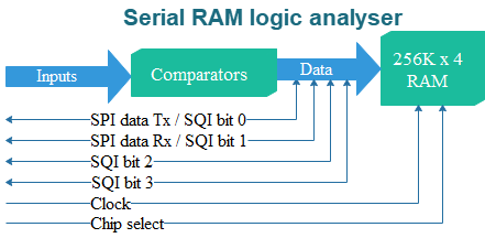
Each RAM chip handles 4 input channels, so 4 chips are needed for the 16-channel input.
The following steps are needed for data capture:
- Send command to switch RAM from SPI to SQI mode
- Send a ‘write’ command, with the desired starting address
- Assert the chip select line, and start the clock signal.
- When capture is complete, stop the clock signal
- Negate chip select, which completes the ‘write’ command
Readback of the captured data is similar, except that a ‘read’ command is used.
Unfortunately there is no way to read back the address counter within the RAM chip, so to keep track of the sampling process, it is necessary to attach a pulse counter to the clock line; a counter/timer within the microcontroller can be used for this purpose.
Another issue is the fact that the RAM data lines serve two purposes; to receive data from the comparators, and commands from the CPU. Ideally the comparators would have an ‘enable’ pin to tri-state their outputs, but I couldn’t find a suitable device with this feature. Failing that, the conventional approach would be to use multiplexer chips to switch between the two data sources, but I’ve taken a much simpler approach, using resistors in the output of the comparators. When the CPU is in control, it just sets the data lines high or low as required, overriding the comparator outputs; when capturing data, the CPU sets its pins as inputs, so the comparators control the data going into the RAM, albeit with a small delay due to the 1K series resistance interacting with the circuit capacitance, but this hasn’t proved a problem in practice.
Triggering
An important feature of logic analysers is triggering; the ability to continuously capture data until a specific condition is met, carry on capturing for a specific number of samples after the trigger, then stop.
The logic to support this operation can be quite complex, and the addition of digital comparators (or their equivalent in programmable logic) would be a major complication. However, it is worth bearing in mind two things:
- If there is a small time-delay between the trigger condition being detected, and the hardware reacting to the trigger, then it is no problem; if we are capturing tens of thousands of samples, a trigger delay of 10 or 20 samples is of no great concern.
- The CPU is largely idle while data is being captured; it only has to respond to network requests, which are largely handled by the 2nd CPU in a dual-CPU device.
In common with most modern microcontrollers, the ESP32 has the ability to generate an interrupt on the state-change of any I/O pin, and this interrupt can be used for triggering, since it can capture very short pulses (under 50 nanoseconds). In theory it is possible to chain several edge-interrupts together, to give more complex triggering, but personally I’ve found a single edge-trigger to be sufficient for most purposes.
ESP32
The decision to use an ESP32 processor was largely driven by its built-in WiFi interface, and the ready availability of complete low-cost modules with a built-in antenna (or connector for an external antenna). The module used is the ESP32-S2-DevKitC with 38 pins, and an ESP32-WROOM-32D or -32E processor; take care not not to be confuse it with similar-looking modules.

This module has a few features that make it an excellent choice:
- Fast dual-CPU architecture.
- Easy-to-use C software development environment based on the VScode IDE, PlatformIO configuration, and the Arduino run-time environment.
- A pin multiplexer that removes a lot of constraints as to which pins can be used for which internal functions
- Simple PWM generator that can generate the required clock frequencies
- Edge-detection interrupts on any I/O pin.
However, there are some less-than-ideal features:
- Gaps in the I/O pin assignments, so it is impossible to assign 8 consecutive bits to form a single byte-wide input, or 16 consecutive bits to form a word-wide input.
- Absence of a general-purpose 32-bit pulse counter; only 16 bits are available.
- Usage of some I/O pins to specify boot-time settings.
- Some GPIO pins are input-only.
These issues can be resolved in software, as will be described in the next blog post, but the final design does use all the input/output pins, with none spare, which forces some economies. For example, it is highly desirable to have a diagnostic LED controlled by the CPU, but there is no O/P pin to drive it, so it has been put on the RAM chip-select line, which slightly reduces the flexibility of the LED indications.
Analog inputs
Each analog input requires an attenuator to reduce the input voltage down to something manageable, and a comparator that compares the attenuated signal with a programmable reference voltage produced by a DAC (Digital-Analog Converter).
The attenuator is just a resistive potential divider; the resistors have been arranged in groups of 8, such that dual-in-line (DIL) plug-in resistor packs can be used in place of discrete resistors. This means that the board can handle very a wide range of input voltages by plugging in different resistor packs.
It proved quite difficult to find a comparator that is readily available, fast enough, and with a push-pull output (not open-drain). An early candidate was the MAX942, but this has back-to-back diodes between the inverting and non-inverting inputs, which would cause major problems if the voltage difference was sufficiently high to make them conduct. In the end, TS3022 devices in SO-8 packages were selected, and they perform really well; provision had been made for adding positive feedback to provide hysteresis (by adding resistors to the DIL-footprint through-holes), but in practice this has not been necessary.

Programming
The ESP32 module has a micro USB connector to provide power to the unit, and a programming interface. As a backup, the PCB also includes a JTAG programming interface, but this uses some of the data pins, so is only usable on a bare depopulated PCB.
The USB interface also emulates a serial console, that is compatible with standard PC terminal emulators; the ESP32 firmware makes extensive use of this for diagnostic reporting.
PCB design
The circuit diagram, PCB manufacturing files (Gerbers) and parts list are in the project repository; do check the README file for the latest information.
The PCB has dual-footprints (DIL & SO-8) for the memory chips and the comparators. I have used DIL sockets for the RAM chips so they can be upgraded at a future date, but as mentioned above, none of the DIL-packaged comparators were suitable, so surface-mount TS3022 parts were used – they have a relatively generous pin spacing (1.27 mm) so shouldn’t be difficult for anyone to assemble who has reasonable soldering skills.
The photo above shows socketed resistor packs for the input attenuators; if using these (as opposed to individual resistors) make sure you buy the type with 8 individual resistors, not commoned.
The ESP32 module requires two 19-way sockets with square pins; I had to use 20-pin parts, with one pin cut off. To help with hardware diagnostics, I have included convenient 2.54 mm pitch headers for the RAM clock, chip select and data lines. These only need to be populated if you are using a logic analyser to trace the board’s operation, or if you wish to remove the ESP32 module and drive the board from some other CPU.
Power (5 volts, with a current capacity of at least 250 mA) is either applied on the USB connector, or on P14, in which case there needs to be an on/off switch connected to the terminals of P7, or those pins must be bonded across. The module is programmed over USB; do not use the JTAG interface unless the board is de-populated.
Part 2 of this project looks at the ESP32 firmware, part 3 the Web interface and Python API. The circuit diagram and PCB files are on Github.
Copyright (c) Jeremy P Bentham 2022. Please credit this blog if you use the information or software in it.
