This is the second part of a 3-part blog post describing a low-cost WiFi-based logic analyser, that can be used for monitoring equipment in remote or hazardous locations. Part 1 described the hardware, this post now describes the firmware within the logic analyser unit.
Development environment
There are two main development environments for the ESP32 processor; ESP-IDF and Arduino-compatible. The former is much more comprehensive, but a lot of those features aren’t needed, so to save time, I have used the latter.
There are two ways of developing Arduino code; using the original Arduino IDE, or using Microsoft Visual Studio Code (VS Code) with a build system called PlatformIO. I originally tried to support both, but found the Arduino IDE too restrictive, so opted for VS Code and PlatformIO.
Installing this on Windows is remarkably easy, see these posts on PlatformIO installation or PlatformIO development
Then it is just necessary to open a directory containing the project files, and after a suitable pause while the necessary files are downloaded, the source files can be compiled, and the resulting binary downloaded onto the ESP32 module.

The code has two main areas: driving the custom hardware that captures the samples, and the network interface.
Hardware driver
As described in the previous post, the main hardware elements driven by the CPU are:
- 16-bit data bus for the RAM chips and the comparator outputs
- Clock & chip select for RAM chips
- SPI interface for the DAC that sets the threshold
Data bus
The sample memory consists of four 23LC1024 serial RAM chips, each storing 1 Mbit in quad-SPI (4-bit) mode. They are arranged to form a 16-bit data bus; it would be really convenient if this could be assigned to 16 consecutive I/O bits on the CPU, but the ESP32 hardware does not permit this. The assignment is:
Data line 0  1  2  3  4  5  6  7  8  9 10 11 12 13 14 15
GPIO      4  5 12 13 14 15 16 17 18 19 21 22 23 25 26 27
There is an obvious requirement to handle the data bus as a single 16-bit value within the code, so it is necessary to provide functions that convert that 16-bit data into a 32-bit value to be fed to the I/O pins, and vice-versa, and it’d be helpful if this was done in an easy-to-understand manner, to simplify any changes when a new CPU is used that has a different pin assignment.
After having tried the usual mess of shift-and-mask operations, I hit upon the idea of creating a bitfield for each group of consecutive GPIO pins, and a matching bitfield for the same group in the 16-bit word; then it is only necessary to equate each field to its partner, to produce the required conversion.
// Data bus pin definitions
// z-variables are unused pins
typedef struct {
    uint32_t z1:4, d0_1:2, z2:6, d2_9:8, z3:1, d10_12:3, z4:1, d13_15:3;
} BUSPINS;
typedef union {
    uint32_t val;
    BUSPINS pins;
} BUSPINVAL;

// Matching elements in 16-bit word
typedef struct {
    uint32_t d0_1:2, d2_9:8, d10_12:3, d13_15:3;
} BUSWORD;
typedef union {
    uint16_t val;
    BUSWORD bits;
} BUSWORDVAL;

// Return 32-bit bus I/O value, given 16-bit word
inline uint32_t word_busval(uint16_t val) {
    BUSWORDVAL w = { .val = val };
    BUSPINVAL  p = { .pins = { 0, w.bits.d0_1,   0, w.bits.d2_9,
                               0, w.bits.d10_12, 0, w.bits.d13_15 } };
    return (p.val);
}

// Return 16-bit word, given 32-bit bus I/O value
inline uint16_t bus_wordval(uint32_t val) {
    BUSPINVAL  p = { .val = val };
    BUSWORDVAL w = { .bits = { p.pins.d0_1, p.pins.d2_9,
                               p.pins.d10_12, p.pins.d13_15 } };
    return (w.val);
}
An additional complication is that the 16-bit value is going to 4 RAM chips, and each chip needs to receive the same command, and the bit-pattern of that command changes depending on whether the chip is in SPI or quad-SPI (QSPI, also known as SQI) mode. So the command to send a command to all 4 RAM chips in SPI mode is:
#define RAM_SPI_DOUT    1
#define MSK_SPI_DOUT    (1 << RAM_SPI_DIN)
#define ALL_RAM_WORD(b) ((b) | (b)<<4 | (b)<<8 | (b)<<12)
uint32_t spi_dout_pins = word_busval(ALL_RAM_WORD(MSK_SPI_DOUT));

// Send byte command to all RAMs using SPI
// Toggles SPI clock at around 7 MHz
void bus_send_spi_cmd(byte *cmd, int len) {
    GPIO.out_w1ts = spi_hold_pins;
    while (len--) {
        byte b = *cmd++;
        for (int n = 0; n < 8; n++) {
            if (b & 0x80) GPIO.out_w1ts = spi_dout_pins;
            else GPIO.out_w1tc = spi_dout_pins;
            SET_SCK;
            b <<= 1;
            CLR_SCK;
        }
    }
}
I have used a ‘bit-bashing’ technique (i.e. manually driving the I/O pins high or low) since I’m emulating 4 SPI transfers in parallel, and as you can see from the comment, the end-result is reasonably fast.
When the RAMS are in QSPI mode, instead of doing eight single-bit transfers, we must do two four-bit transfers:
// Send a single command to all RAMs using QSPI
void bus_send_qspi_cmd(byte *cmd, int len) {
    while (len--) {
        uint32_t b1=*cmd>>4, b2=*cmd&15;
        uint32_t val=word_busval(ALL_RAM_WORD(b1));
        gpio_out_bus(val);
        SET_SCK;
        val = word_busval(ALL_RAM_WORD(b2));
        CLR_SCK;
        gpio_out_bus(val);
        SET_SCK;
        cmd++;
        CLR_SCK;
    }
}
The above code assumes that the appropriate I/O pin-directions (input or output) have been set, but that too depends on which mode the RAMs are in; for SPI each RAM chip has 2 data inputs (DIN and HOLD) and 1 output (DOUT), whilst in QSPI mode all 4 RAM data pins are inputs or outputs depending on whether the RAM is being written to, or read from.
There are 4 commands that the software sends to the RAM chips, each is a single byte:
- 0x38: enter quad-SPI (QSPI) mode
- 0xff: leave QPSI mode, enter SPI mode
- 0x02: write data
- 0x03: read data
The read & write commands are followed by a 3-byte address value, that dictates the starting-point for the transfer. So if the RAMs are already in QSPI mode, the sequence for capturing samples is:
- Set bus pins as outputs, so bus is controlled by CPU
- Assert RAM chip select
- Send command byte, with a value of 2 (write)
- Send 3 address bytes (all zero when starting data capture)
- Set bus pins as inputs, so bus is controlled by comparators
- Start RAM clock
- When capture is complete, stop RAM clock
- Negate RAM chip select
The steps for recovering the captured data are:
- Set bus pins as outputs, so bus is controlled by CPU
- Assert RAM chip select
- Send command byte, with a value of 3 (read)
- Send 3 address bytes
- Set bus pins as inputs, so bus is controlled by the RAM chips
- Toggle clock line, and read data from the 16-bit bus
- When readout is complete, negate RAM chip select
RAM clock and chip select
When the CPU is directly accessing the RAM chips (to send commands, or read back data samples) it is most convenient to ‘bit-bash’ the clock and I/O signals, as described above. It is possible that incoming interrupts can cause temporary pauses in the clock transitions, but this doesn’t matter: the RAM chips use ‘static’ memory, which won’t change its state even if there is a very long pause in a transfer cycle.
However, when capturing data, it is very important that the RAMs receive a steady clock at the required sample rate, with no interruptions. This is easily achieved on the ESP32 by using the LED PWM peripheral:
#define PIN_SCK         33
#define PWM_CHAN        0

// Initialise PWM output
void pwm_init(int pin, int freq) {
    ledcSetup(PWM_CHAN, freq, 1);
    ledcAttachPin(pin, PWM_CHAN);
}

// Start PWM output
void pwm_start(void) {
    ledcWrite(PWM_CHAN, 1);
}
// Stop PWM output
void pwm_stop(void) {
    ledcWrite(PWM_CHAN, 0);
}
In addition, the CPU must count the number of pulses that have been output, so that it knows which memory address is currently being written – there is no way to interrogate the RAM chip to establish its current address value. Surprisingly, the ESP32 doesn’t have a general-purpose 32-bit counter, so we have to use the 16-bit pulse-count peripheral instead, and detect overflows in order to produce a 32-bit value.
volatile uint16_t pcnt_hi_word;

// Handler for PCNT interrupt
void IRAM_ATTR pcnt_handler(void *x) {
    uint32_t intr_status = PCNT.int_st.val;
    if (intr_status) {
        pcnt_hi_word++;
        PCNT.int_clr.val = intr_status;
    }
}

// Initialise PWM pulse counter
void pcnt_init(int pin) {
    pcnt_intr_disable(PCNT_UNIT);
    pcnt_config_t pcfg = { pin, PCNT_PIN_NOT_USED, PCNT_MODE_KEEP, PCNT_MODE_KEEP,
        PCNT_COUNT_INC, PCNT_COUNT_DIS, 0, 0, PCNT_UNIT, PCNT_CHAN };
    pcnt_unit_config(&pcfg);
    pcnt_counter_pause(PCNT_UNIT);
    pcnt_event_enable(PCNT_UNIT, PCNT_EVT_THRES_0);
    pcnt_set_event_value(PCNT_UNIT, PCNT_EVT_THRES_0, 0);
    pcnt_isr_register(pcnt_handler, 0, 0, 0);
    pcnt_intr_enable(PCNT_UNIT);
    pcnt_counter_pause(PCNT_UNIT);
    pcnt_counter_clear(PCNT_UNIT);
    pcnt_counter_resume(PCNT_UNIT);
    pcnt_hi_word = 0;
}

// Return sample counter value (mem addr * 2), extended to 32 bits
uint32_t pcnt_val32(void) {
    uint16_t hi = pcnt_hi_word, lo = PCNT.cnt_unit[PCNT_UNIT].cnt_val;
    if (hi != pcnt_hi_word)
        lo = PCNT.cnt_unit[PCNT_UNIT].cnt_val;
    return(((uint32_t)hi<<16) | lo);
}
When writing this code, I came across some strange features of the PCNT interrupt, such as multiple interrupts for a single event, and misleading values when reading the count value inside the interrupt handler, so be careful when doing any modifications.
The pulse count does not equal the RAM address; is the RAM address multiplied by 2. This is because it takes two 4-bit write cycles to create one byte in RAM (bits 4-7, then 0-3), so the memory chip increments its RAM address once for every 2 samples.
All the RAMs share a single clock line and chip select; the select line is driven low at the start of a command, and must remain low for the duration of the command and data transfer; when it goes high, the transfer is terminated.
Setting threshold value
The comparators compare the incoming signal with a threshold value, to determine if the value is 1 or 0 (above or below threshold). The threshold is derived from a digital-to-analog converter (DAC), the part I’ve chosen is the Microchip MCP4921; it was necessary to use a part with an SPI interface, since there is only 1 spare output pin, which serves as the chip select for this device; the clock and data pins are shared with the RAM chips.
This means that the DAC control code can use the same drivers as the RAM chips by negating the RAM chip select, and asserting the DAC chip select:
#define PIN_DAC_CS      2
#define DAC_SELECT      GPIO.out_w1tc = 1<<PIN_DAC_CS
#define DAC_DESELECT    GPIO.out_w1ts = 1<<PIN_DAC_CS

// Output voltage from DAC; Vout = Vref * n / 4096
void dac_out(int mv) {
    uint16_t w = 0x7000 + ((mv * 4096) / 3300);
    byte cmd[2] = { (byte)(w >> 8), (byte)(w & 0xff) };
    RAM_DESELECT;
    DAC_SELECT;
    bus_send_spi_cmd(cmd, 2);
    DAC_DESELECT;
}
Triggering
Triggering is achieved by using the ESP32 pin-change interrupt, as this can capture quite a narrow pulses. There will be a delay before the interrupt is serviced, which means that we don’t get an accurate indication of which sample caused the trigger, but that isn’t a problem in practice.
int trigchan, trigflag;

// Handler for trigger interrupt
void IRAM_ATTR trig_handler(void) {
    if (!trigflag) {
        trigsamp = pcnt_val32();
        trigflag = 1;
    }
}

// Enable or disable the trigger interrupt for channels 1 to 16
void set_trig(bool en) {
    int chan=server_args[ARG_TRIGCHAN].val, mode=server_args[ARG_TRIGMODE].val;
    if (trigchan) {
        detachInterrupt(busbit_pin(trigchan-1));
        trigchan = 0;
    }
    if (en && chan && mode) {
        attachInterrupt(busbit_pin(chan-1), trig_handler,
            mode==TRIG_FALLING ? FALLING : RISING);
        trigchan = chan;
    }
    trigflag = 0;
}
This interrupt handler sets a flag, that is actioned by the main state machine. There is a ‘trig_pos’ parameter that sets how many tenths of the data should be displayed prior to triggering; it is normally set to 1, which means that (approximately) 1 tenth will be displayed before the trigger, and 9 tenths after.
It is possible that there may be a considerable delay before the trigger event is encountered. In this case, the unit continues to capture samples, and the RAM address counter will wrap around every time it reaches the maximum value. This means that the pre-trigger data won’t necessarily begin at address zero; the firmware has to fetch the trigger RAM address, then jump backwards to find the start of the data.
State machine
This handles the whole capture process. There are 6 states:
- Idle: no data, and not capturing data
- Ready: data has been captured, ready to be uploaded
- Preload: capturing data, before looking for trigger
- PreTrig: capturing data, looking for trigger
- PostTrig: capturing data after trigger
- Upload: transferring data over the network
The Preload state is needed to ensure there is some data prior to the trigger. If triggering is disabled, then as soon as the capture is started, the software goes directly to the PostTrig state, checking the sample count to detect when it is greater than the requested number.
// Check progress of capture, return non-zero if complete
bool web_check_cap(void) {
    uint32_t nsamp = pcnt_val32(), xsamp = server_args[ARG_XSAMP].val;
    uint32_t presamp = (xsamp/10) * server_args[ARG_TRIGPOS].val;
    STATE_VALS state = (STATE_VALS)server_args[ARG_STATE].val;
    server_args[ARG_NSAMP].val = nsamp;
    if (state == STATE_PRELOAD) {
        if (nsamp > presamp)
            set_state(STATE_PRETRIG);
    }
    else if (state == STATE_PRETRIG) {
        if (trigflag) {
            startsamp = trigsamp - presamp;
            set_state(STATE_POSTTRIG);
        }
    }
    else if (state == STATE_POSTTRIG) {
        if (nsamp-startsamp > xsamp) {
            cap_end();
            set_state(STATE_READY);
            return(true);
        }
    }
    return (false);
}
Network interface
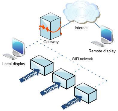
A detailed description of network operation will be found in part 3 of this project; for now, it is sufficient to say that the unit acts as a wireless client, connecting to a pre-defined WiFi access point; it has a simple Web server with all requests & responses using HTTP.
Wireless connection
The first step is to join a wireless network, using a predefined network name (‘SSID’) and password. The code must also try to re-establish the link to he Access Point if the connection fails, so there is a polling function that checks for connectivity.
// Begin WiFi connection
void net_start(void) {
    DEBUG.print("Connecting to ");
    DEBUG.println(ssid);
    WiFi.begin(ssid, password);
    WiFi.setSleep(false);
}

// Check network is connected
bool net_check(void) {
    static int lastat=0;
    int stat = WiFi.status();
    if (stat != lastat) {
        if (stat<=WL_DISCONNECTED) {
            DEBUG. printf("WiFi status: %s\r\n", wifi_states[stat]);
            lastat = stat;
        }
        if (stat == WL_DISCONNECTED)
            WiFi.reconnect();
    }
    return(stat == WL_CONNECTED);
}
Web server
The Web pages are very simple and only contain data; the HTML layout and Javascript code to display the data is fetched from a different server.
The server is initialised with callbacks for three pages:
#define STATUS_PAGENAME "/status.txt"
#define DATA_PAGENAME   "/data.txt"
#define HTTP_PORT       80

WebServer server(HTTP_PORT);

// Check if WiFi & Web server is ready
bool net_ready(void) {
    bool ok = (WiFi.status() == WL_CONNECTED);
    if (ok) {
        DEBUG.print("Connected, IP ");
        DEBUG.println(WiFi.localIP());
        server.enableCORS();
        server.on("/", web_root_page);
        server.on(STATUS_PAGENAME, web_status_page);
        server.on(DATA_PAGENAME, web_data_page);
        server.onNotFound(web_notfound);
        DEBUG.print("HTTP server on port ");
        DEBUG.println(HTTP_PORT);
        delay(100);
    }
    return (ok);
}
The root page returns a simple text string, and is mainly used to check that the Web server is functioning:
#define HEADER_NOCACHE  "Cache-Control", "no-cache, no-store, must-revalidate"

// Return root Web page
void web_root_page(void) {
    server.sendHeader(HEADER_NOCACHE);
    sprintf((char *)txbuff, "%s, attenuator %u:1", version, THRESH_SCALE);
    server.send(200, "text/plain", (char *)txbuff);
}
All the Web pages are sent with a header that disables browser caching; this is necessary to ensure that the most up-to-date data is displayed.
The status page returns a JSON (Javascript Object Notation) formatted string, containing the current settings; a typical response might be:
{"state":1,"nsamp":10010,"xsamp":10000,"xrate":100000,"thresh":10,"trig_chan":0,"trig_mode":0,"trig_pos":1}
This indicates that 10000 samples were requested at 100 KS/s, 10010 were actually collected, using a threshold of 10 volts. The ‘state’ value of 1 indicates that data collection is complete, and the data is ready to be uploaded.
The individual arguments are stored in an array of structures, which is converted into the JSON string:
typedef struct {
    char name[16];
    int val;
} SERVER_ARG;

SERVER_ARG server_args[] = {
    {"state",       STATE_IDLE},
    {"nsamp",       0},
    {"xsamp",       10000},
    {"xrate",       100000},
    {"thresh",      THRESH_DEFAULT},
    {"trig_chan",   0},
    {"trig_mode",   0},
    {"trig_pos",    1},
    {""}
};

// Return server status as json string
int web_json_status(char *buff, int maxlen) {
    SERVER_ARG *arg = server_args;
    int n=sprintf(buff, "{");
    while (arg->name[0] && n<maxlen-20) {
        n += sprintf(&buff[n], "%s\"%s\":%d", n>2?",":"", arg->name, arg->val);
        arg++;
    }
    return(n += sprintf(&buff[n], "}"));
}
The HTTP request for the status page can also include a query string with parameters that reflect the values the user has entered in a Web form. If a ‘cmd’ parameter is included, it is interpreted as a command; the following query includes ‘cmd=1’, which starts a new capture:
GET /status.txt?unit=1&thresh=10&xsamp=10000&xrate=100000&trig_mode=0&trig_chan=0&zoom=1&cmd=1
The software matches the parameters with those in the server_args array, and stores the values in that array; unmatched parameters (such as the zoom level) are ignored.
// Return status Web page
void web_status_page(void) {
    web_set_args();
    web_do_command();
    web_json_status((char *)txbuff, TXBUFF_LEN);
    server.sendHeader(HEADER_NOCACHE);
    server.setContentLength(CONTENT_LENGTH_UNKNOWN);
    server.send(200, "application/json");
    server.sendContent((char *)txbuff);
    server.sendContent("");
}

// Get command from incoming Web request
int web_get_cmd(void) {
    for (int i=0; i<server.args(); i++) {
        if (!strcmp(server.argName(i).c_str(), "cmd"))
            return(atoi(server.arg(i).c_str()));
    }
    return(0);
}

// Get arguments from incoming Web request
void web_set_args(void) {
    for (int i=0; i<server.args(); i++) {
        int val = atoi(server.arg(i).c_str());
        web_set_arg(server.argName(i).c_str(), val);
    }
}
Data transfer
The captured data is transferred using an HTTP GET request to the page data.txt. The binary data is encoded using the base64 method, which converts 3 bytes into 4 ASCII characters, so it can be sent as a text block. There is insufficient RAM in the ESP32 to store the sample data, so it is transferred on-the-fly from the RAM chips to a network buffer.
// Return data Web page
void web_data_page(void) {
    web_set_args();
    web_do_command();
    server.sendHeader(HEADER_NOCACHE);
    server.setContentLength(CONTENT_LENGTH_UNKNOWN);
    server.send(200, "text/plain");
    cap_read_start(startsamp);
    int count=0, nsamp=server_args[ARG_XSAMP].val;
    size_t outlen = 0;
    while (count < nsamp) {
        size_t n = min(nsamp - count, TXBUFF_NSAMP);
        cap_read_block(txbuff, n);
        byte *enc = base64_encode((byte *)txbuff, n * 2, &outlen);
        count += n;
        server.sendContent((char *)enc);
        free(enc);
    }
    server.sendContent("");
    cap_read_end();
}
The ‘unknown’ content length means that the software can send an arbitrary number of text blocks, without having to specify the total length in advance. The transfer is terminated by calling sendContent with a null string.
Diagnostics
There is a single red LED, but due to pin constraints, it is shared with the RAM chip select. So it will always illuminate when the RAM is being accessed, but in addition:
- Rapid flashing (5 Hz) if the unit is not connected to the WiFi network
- Brief flash (100 ms every 2 seconds) when the unit is connected to the network.
- Solid on when the unit is capturing data, and is waiting for a trigger, or until the required amount of data has been collected.
There is also the ESP32 USB interface that emulates a serial console at 115 Kbaud:
#define DEBUG_BAUD  115200
#define DEBUG       Serial      // Debug on USB serial link

DEBUG.begin(DEBUG_BAUD);

// 'print' 'println' and 'printf' functions are supported, e.g.
DEBUG.print("Connecting to ");
DEBUG.println(ssid);
To view the console display, you can use your favourite terminal emulator (e.g. TeraTerm on Windows) connected to the USB serial port, however you will have to break that connection every time you re-program the ESP32, since it is needed for re-flashing the firmware. The VS Code IDE does have its own terminal emulator, which generally auto-disconnects for re-programming, but I have had occasional problems with this feature, for reasons that are a bit unclear.
Modifications
There are a few compile-time options that need to be set before compiling the source code:
- SW_VERSION (in main.cpp): a string indicating the current software version number
- ssid & password (in esp32_web.cpp): must be changed to match your wireless network
- THRESH_SCALE (in esp32_la.h): the scaling factor for the threshold value, that is used to program the DAC.
The threshold scaling will depend on the values of the attenuator resistors. The unit was originally designed for input voltages up to 50V, with a possible overload to 250V, so the input attenuation was 101 (100K series resistor, 1K shunt resistor). If using the unit with, say, 5 volt logic, then the series resistor will need to be much lower (and maybe the shunt resistance a bit higher) so the threshold scaling value will need to be adjusted accordingly. Since the threshold value sent from the browser is an integer value (currently 0 – 50) you might choose the redefine that value when working with lower voltages, for example represent 0 – 7 volts as a value of 0 – 70, in tenths of a volt. This change will need to be made in the firmware, and both Web interfaces.
An important note, when creating a new unit. Since I’m using all the available I/O pins on the ESP32, I’ve had to use GPIO12, even though this does (by default) determine the Flash voltage at startup.
To use the pin for I/O, it is essential that this behaviour is changed by modifying the parameters in the ESP32 one-time-programmable memory. This is done using the Python espefuse program that is provided in the IDE. To summarise the current settings, navigate to the directory containing that file, and execute:
python espefuse.py --port COM4 summary
..assuming the USB serial link is on Windows COM port 4. Then to modify the setting, execute:
python espefuse.py --port COM4 set_flash_voltage 3.3V
You will be prompted to confirm that the change should be made, since it is irreversible. Then if you re-run the summary, the last line should be:
Flash voltage (VDD_SDIO) set to 3.3V by efuse.
Part 1 of this project looked at the hardware, part 3 the Web interface and Python API. The source files are on Github.
Copyright (c) Jeremy P Bentham 2022. Please credit this blog if you use the information or software in it.
