To debug embedded systems, such as those with the Raspberry Pi Pico processor, normally only two options are available: using ‘print’ statements, or a debug utility such as GDB. This project offers an alternative, which isn’t as invasive as the ‘print’ method, and isn’t as complex as GDB. It basically provides an insight as to the functioning of the processor and peripherals, while they are running – the CPU need not be halted to do the measurements, and the indications are equally relevant for C or Python programs.
Sadly, I can’t promise that this utility will automatically find bugs in your code; in operation, it is more like a test meter that is used to check the voltages and currents in an electrical circuit; it will show you what is going on, and give you pointers to the hardware or software areas that might be malfunctioning.
There are major differences between the on-chip debug resources for the RP2040 and RP2350; the latter is far more complex, with the potential for using much more sophisticated debug techniques. However, at the time of writing, the RP2350 is still quite a new processor, and has not yet achieved widespread usage. So the current version of PicoReg concentrates on debug features that are common to both devices; later versions will make use of the advanced features of the RP2350 to provide more sophisticated debug capabilities.
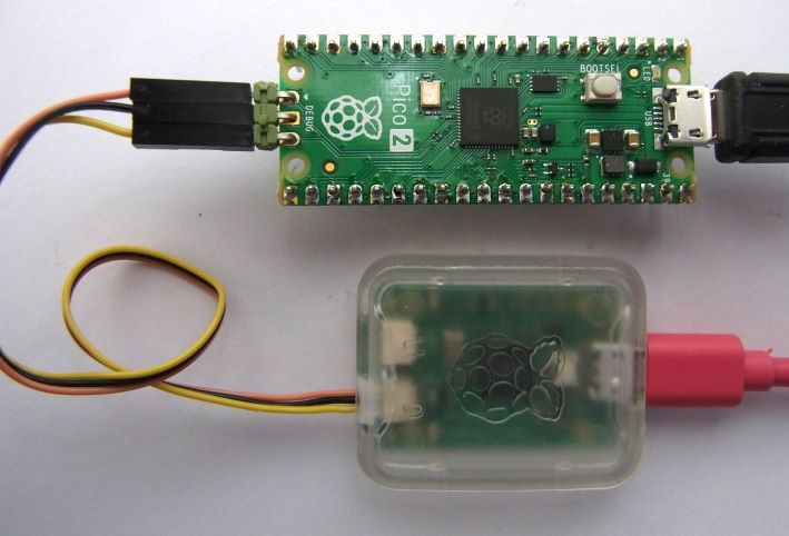
For ease of use, the PicoReg utility is written in pure Python, so it will run on a Windows or Linux PC, or a Raspberry Pi board. The interface to the target CPU is via the standard low-cost Raspberry Pi Debug Probe, with a USB interface to the PC or Pi, and a 3-wire SWD interface to the target system.
Connecting the target system
Connect the target system to the debug probe as described in the Raspberry Pi documentation, either using a 3-pin 0.1 inch pitch header as shown above, or the 3-pin miniature JST connector that is fitted to the ‘H’ variants of the Pico boards (e.g. RP2040H). It is important to keep the SWD cable short, ideally a maximum of 6 inches or 15 cm, with a good ground connection, since the signals are quite fast (10 MHz).
The Pi Debug Probe has an ARM-standard ‘CMSIS-DAP’ USB interface, and you can find other low-cost CMSIS-DAP probes online, however they probably won’t work without significant modifications to the Python code, so are not recommended.
A benefit to this setup is that it is exactly the same as used with OpenOCD, so is compatible with all the standard Pico software tools; you don’t need to re-plug the target system when switching between programming and debugging.
Installing PicoReg
The source code can be found on github here and can be copied into any convenient directory.
The files are:
picoreg.py:            main program
picoreg_disp.py:       display code
picoreg_swd.py:        SWD interface
picoreg_arm.py:        ARM CPU interface
rp2040.svd:            ARM register definitions for RP2040
rp2350.svd:            ARM register definitions for RP2350
icons/led_red_off.png: icon for I/O display
icons/led_red_on.png:  icon for I/O display
The register definition files have been taken directly from the Pico SDK, and have been provided as a convenience; they can be replaced with more up-to-date versions from the SDK, but do ensure the filenames are all in lower-case.
It is necessary to install PyQt5, pyusb, and libusb_package, e.g. for Linux:
If debug probe lacks the necessary access permission, create /etc/udev/rules.d/50-usb-cmsis.rules with the following line: SUBSYSTEM=="usb", ATTR{idVendor}=="2e8a", ATTRS{idProduct}=="000c", MODE="0666"
On newer Linux systems, the pip install method may fail with the error message “This environment is externally managed” . You can find guidance online as to the correct method of handling this error; the simplest way is to override package management by appending ‘–break-system-packages’ to the pip command.
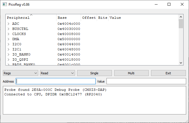
To check the USB connection to the probe, and the SWD connection to the CPU, run
python picoreg_swd.py
The response should be:
If working OK:
Found debug probe (CMSIS-DAP)
CPU ID 0BC12477 [for RP2040, or 4C013477 for RP2350]

If target board disconnected or powered down:
Target not responding

If debug probe not connected:
Probe not found
The code can be run on any Pi Linux system, but it is recommended that a Pi4 or later be used, otherwise the user interface may be a bit sluggish.
Running PicoReg
PicoReg is run using:
python picroreg.py
If all is well, the CPU type (RP2040 / RP2350) should be auto-detected, the appropriate SVD definition file will be parsed, and displayed in tree format.
By default, the peripheral names are sorted alphabetically; clicking on another heading will change the sorting, e.g. ‘base’ to sort by base address.
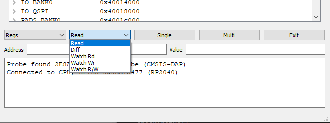
The first control (showing ‘Regs’) has a drop-down list of the various operational modes:
Regs:   Show all the CPU registers in tree format
I/O:    Display the on/off state and mode of the I/O pins
CPU:    View some of the CPU registers
Mem:    Display a block of memory or registers at a given address
PIO:    Show some of the PIO-specific registers
DMA:    Show some of the DMA-specific registers
The Regs, PIO and DMA modes are very similar, only differing in the number of registers on display. Regs mode displays the full set as defined in the SVD file, the other 2 modes show only a subset, which can make it easier to understand the operation of the selected peripheral.
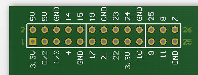
The I/O display uses LED icons and text to display the state of all 29 I/O pins:
This shows the display for a typical ‘blinking LED’ program; the on-board LED on pin 25 blinks on and off, under the control of the SIO peripheral. The only other pins being controlled are pin 0 and 1, which are under the control of UART0 (asynchronous serial transmit and receive).
CPU mode shows some of the processor registers, which can be useful to check that it is running (not crashed) and give an indication of activity.
This shows that the code is running in Flash memory (10000000 hex onwards) with the stack in RAM (20000000 hex onwards).
Mem mode is used to display arbitrary areas of memory or registers (since the registers are memory-mapped).
This shows a small block of RAM that acting as a WiFi data buffer.
The second drop-down list selects the access mode:
Read:      Display read value
Diff:      Add the current value to a list, when the value changes
Watch Rd:  Set data watchpoint, display data on CPU write cycle
Watch Rd:  Set data watchpoint, display data on CPU read cycle
Watch R/W: Set data watchpoint, display data when CPU read or write cycle
The Read and Diff modes rely on continuous polling of the target system, at approximately 1000 times per second, so they can not capture fast changing signals. The Watch modes use the CPU hardware to detect changes, so a single rapid change will be detected, but there is a finite delay before the PC can capture the data values and re-check for another change, so multiple rapid events will not all be captured.
The ‘single’ button does one read cycle, and the ‘multi’ button runs continuous cycles until that button is pressed again.
Command-line options
Running ‘python picoreg.py -h’ produces the following help:
optional arguments: -h, --help show this help message and exit -b, --break RP2350 break on watchpoint -m MEM, --mem MEM Memory address -n NBYTES, --nbytes NBYTES Number of bytes for hex dump -r REG, --reg REG Register name -v, --verbose Enable diagnostic display -2, --core2 Use second core
The options are:
break: force the RP2350 to do a brief break on each watchpoint making its behaviour similar to the RP2040, which has to break on each watchpoint.
mem: add a specific memory address to the display. This is useful when working with a C program; the compiler generates a map file with the address of all global variables, and this option can be used (one or more times) to add addresses to the display.
nbytes: set the number of bytes to be displayed on a memory dump, the default value is 32.
reg: select a specific register to be monitored. This is case-sensitive e.g. TIMER.TIMERAWL for RP2040, or TIMER0.TIMERAWL for RP2350
verbose: display the raw CMSIS-DAP messages
2: select the second ARM core; the RP2350 RISC-V cores are not currently available
Copyright (c) Jeremy P Bentham 2025. Please credit this blog if you use the information or software in it.
The nRF52832 is an ARM Cortex M4 chip with an impressive range of peripherals, including an on-chip 2.4 GHz wireless transceiver. Nordic supply a comprehensive SDK with plenty of source-code examples; they are fully compatible with the GCC compiler, but there is little information on how to program and debug a target system using open-source tools such as the GDB debugger, or the OpenOCD JTAG/SWD programmer.
This blog will show you how to compile, program and debug some simple examples using the GNU ARM toolchain; the target board is the NRF52832 Breakout from Sparkfun, and the programming is done via a Nordic development board, or OpenOCD on a Raspberry Pi. Compiling & debugging is with GCC and GDB, running on Windows or Linux.
Source files
All the source files are in an ‘nrf_test’ project on GitHub; if you have Git installed, change to a suitable project directory and enter:
git clone https://github.com/jbentham/nrf_test
Alternatively you can download a zipfile from github here. You’ll also need the nRF5 15.3.0 SDK from the Nordic web site. Some directories need to be copied from the SDK to the project’s nrf5_sdk subdirectory; you can save disk space by only copying components, external, integration and modules as shown in the graphic above.
Windows PC hardware
Cortex Debug Connection to a Nordic evaluation board.
The standard programming method advocated by Nordic is to use the Segger JLink adaptor that is incorporated in their evaluation boards, and the Windows nRF Command Line Tools (most notably, the nrfjprog utility) that can be downloaded from their Web site.
Connection between the evaluation board and target system can be a bit tricky; the Sparkfun breakout board has provision for a 10-way Cortex Debug Connector, and adding the 0.05″ pitch header does require reasonable soldering skills. However, when that has been done, a simple ribbon cable can be used to connect the two boards, with no need to change any links or settings from their default values.
One quirk of this arrangement is that the programming adaptor detects the 3.3V power from the target board in order to switch the SWD interface from the on-board nRF52 chip to the external device. This has the unfortunate consequence that if you forget to power up the target board, you’ll be programming the wrong device, which can be confusing.
The JLink adaptor isn’t the only programming option for Windows; you can use a Raspberry Pi with OpenOCD installed…
Raspberry Pi hardware
Raspberry Pi SWD interface (pin 1 is top right in this photo)
In a previous blog, I described the use of OpenOCD on the raspberry Pi; it can be used as a Nordic device programmer, with just 3 wires: ground, clock and data – the reset line isn’t necessary. The breakout board needs a 5 volt supply which could be taken from the RPi, but take care: accidentally connecting a 5V signal to a 3.3V input can cause significant damage.
Rasberry Pi SWD connectionsNRF52832 breakout SWD connections
Install OpenOCD as described in the previous blog; I’ve included the RPi and SWD configuration files in the project openocd directory, so for the RPi v2+, run the commands:
cd nrf_test
sudo openocd -f openocd/rpi2.cfg -f openocd/nrf52_swd.cfg
The response should be..
BCM2835 GPIO config: tck = 25, tms = 24, tdi = 23, tdo = 22

Info : Listening on port 6666 for tcl connections
Info : Listening on port 4444 for telnet connections
Info : BCM2835 GPIO JTAG/SWD bitbang driver
Info : JTAG and SWD modes enabled
Info : clock speed 1001 kHz
Info : SWD DPIDR 0x2ba01477
Info : nrf52.cpu: hardware has 6 breakpoints, 4 watchpoints
Info : Listening on port 3333 for gdb connections
The DPIDR value of 0x2BA01477 is correct for the nRF52832 chip; if any other value appears, there is a problem: check the wiring.
Windows development tools
The recommended compiler toolset for the SDK files is gcc-arm-none-eabi, version 7-2018-q2-update, available here. This places the tools in the directory
C:\Program Files (x86)\GNU Tools Arm Embedded\7 2018-q2-update\bin
Check that this directory in included in your search path by opening a command window, and typing
arm-none-eabi-gcc -v
If not found, close the window, add to the PATH environment variable, and retry.
You will also need to install Windows ‘make’ from here. At the time of writing, the version is 3.81, but I suspect most modern versions would work fine. As with GCC, check that it is included in your executable path by opening a new command window, and typing
make -v
Linux development tools
A Raspberry Pi 2+ is quite adequate for compiling and debugging the test programs.
Although RPi Linux already has an ARM compiler installed, the executable programs it creates are heavily dependant on the operating system, so we also need to install a cross-compiler: arm-none-eabi-gcc version 7-2018-q2-update. The easiest way to do this is to click on Add/Remove software in the Preferences menu, then search for arm-none-eabi. The correct version is available on Raspbian ‘Buster’, but probably not on earlier distributions.
The directory structure is the same as for Windows, with the SDK components, external, integration and modules directories copied into the nrf5_sdk subdirectory.
As with Windows, it is worth typing
arm-none-eabi-gcc -v
..to make sure the GCC executable is installed correctly.
nrf_test1.c
This is in the nrf_test1 directory, and is as simple as you can get; it just flashes the blue LED at 1 Hz.
// Simple LED blink on nRF52832 breakout board, from iosoft.blog

#include "nrf_gpio.h"
#include "nrf_delay.h"

// LED definitions
#define LED_PIN      7
#define LED_BIT      (1 << LED_PIN)

int main(void)
{
    nrf_gpio_cfg_output(LED_PIN);

    while (1)
    {
        nrf_delay_ms(500);
        NRF_GPIO->OUT ^= LED_BIT;
    }
}

// EOF
An unusual feature of this CPU is that the I/O pins aren’t split into individual ports, there is just a single port with a bit number 0 – 31. That number is passed to an SDK function to initialise the LED O/P pin, and I could have used another SDK function to toggle the pin, but instead used an exclusive-or operation on the hardware output register.
The SDK delay function is implemented by performing dummy CPU operations, so isn’t particularly accurate.
Compiling
For both platforms, the method is the same: change directory to nrf_test1, and type ‘make’; the response should be similar to:
Assembling ../nrf5_sdk/modules/nrfx/mdk/gcc_startup_nrf52.S
 Compiling ../nrf5_sdk/modules/nrfx/mdk/system_nrf52.c
 Compiling nrf_test1.c
 Linking build/nrf_test1.elf
    text    data     bss     dec     hex filename
..for Windows..
    1944     108      28    2080     820 build/nrf_test1.elf
..or for Linux..
    2536     112     172    2820     b04 build/nrf_test1.elf
If your compile-time environment differs from mine, it shouldn’t be difficult to change the Makefile definitions to match, but there are some points to note:
The main changeable definitions are towards the top of the file. Resist the temptation to rearrange CFLAGS or LNFLAGS, as this can create a binary image that crashes the target system.
You can add files to the SRC_FILES definition, they will be compiled and linked in; the order of the files isn’t significant, but I generally put gcc_startup_nrf52.S first, so Reset_Handler is at the start of the executable code. Similarly, INC_FOLDERS can be expanded to include any other folders with your .h files.
The task definitions toward the bottom of the file use the tab character for indentation. This is essential: if replaced with spaces, the build process will fail.
ELF, HEX and binary files are produced in the ‘build’ subdirectory; ELF is generally used with GDB, while HEX is required by the JLink flash programmer.
I’ve defined the jflash and ocdflash tasks, that do flash programming after the ELF target is built; you can add your own custom programming environment, using a similar syntax.
The makefile will re-compile any C source files after they are changed, but will not automatically detect changes to the ‘include’ files, or the makefile itself; when these are edited, it will be necessary to force a re-make using ‘make -B’.
If a new image won’t run on the target system, the most common reason is an un-handled exception, and it can be quite difficult to find the cause. So I’d recommend that you expand the code in relatively small steps, making it easier to backtrack if there is a problem.
Device programming
Having built the binary image, we need to program it into Flash memory on the target device. This can be done by:
JLink adaptor on an evaluation board (Windows PC only)
Directly driving OpenOCD (RPi only)
Using the GNU debugger GDB to drive OpenOCD (both platforms)
Device programming using JLink
Set up the hardware and install the Nordic nRF Command Line Tools as described above, then the nrfjflash utility can be used to program the target device with a hex file, e.g.
The second line resets the chip after programming, to start the program running. This is done via the SWD lines, a hardware reset line isn’t required; alternatively you can just power-cycle the target board.
The above commands have been included in the makefile, so if you enter ‘make jflash’, the programming commands will be executed after the binary image is built.
An additional usage of the JLink programmer is to restore the original Arduino bootloader, that was pre-installed on the Sparkfun board. To do this, you need to get hold of the softdevice and DFU files from the Sparkfun repository, combine them using the Nordic merge utility, then program the result using a whole-chip erase:
OpenOCD can be used to directly program the target device, providing the image has been built on the Raspberry Pi, or the ELF file has been copied from the development system. Install and test OpenOCD as described in the Raspberry Pi Hardware section above (check the DPIDR value is correct), hit ctrl-C to terminate it, then enter the command:
 ** Programming Started **
 Info : nRF52832-QFAA(build code: E0) 512kB Flash
 Warn : using fast async flash loader. This is currently supported
 Warn : only with ST-Link and CMSIS-DAP. If you have issues, add
 Warn : "set WORKAREASIZE 0" before sourcing nrf51.cfg/nrf52.cfg to disable it
 ** Programming Finished **
 ** Verify Started **
 ** Verified OK **
 ** Resetting Target **
 shutdown command invoked
Note the warnings: by default, OpenOCD uses a ‘fast async flash loader’ that achieves a significant speed improvement by effectively sending a write-only data stream. Unfortunately the Nordic chip occasionally takes exception to this, and returns a ‘wait’ response, which can’t be handled in fast async mode, so the programming fails – in my tests with small binary images, it does fail occasionally. As recommended in the above text, I’ve tried adding ‘set WORKAREASIZE 0’ to nrf52_swd.cfg (before ‘find target’), but this caused problems when using GDB. By the time you read this, the issue may well have been solved; if not, you might have to do some experimentation to get reliable programming.
The makefile includes the OpenOCD direct programming commands, just run ‘make ocdflash’.
Device programming using GDB and OpenOCD
The primary reason for using GDB is to debug the target program, but it can also serve as a programming front-end for OpenOCD. This method works with PC host, or directly on the RPi, as shown in the following diagram.
GDB OpenOCD debugging
In both cases we are using the GB ‘target remote’ command; on the development PC we have to specify the IP address of the RPi: for example, 192.168.1.2 as shown above. If in doubt as to the address, it is displayed if you hover the cursor over the top-right network icon on the RPi screen. By default, OpenOCD only responds to local GDB requests, so the command ‘bindto 0.0.0.0’ must be added to the configuration. This means anyone on the network could gain control of OpenOCD, so use with care: consider the security implications.
Alternatively, the Raspberry Pi can host both GDB and OpenOCD, in which case the ‘localhost’ address is used, and there is no need for the additional ‘bindto’.
The commands for the PC-hosted configuration are:
# On the RPi:
  sudo openocd -f ../openocd/rpi2.cfg -f ../openocd/nrf52_swd.cfg -c "bindto 0.0.0.0"

# On the Windows PC:
arm-none-eabi-gdb -ex="target remote 192.168.1.2:3333" build\nrf_test1.elf -ex "load" -ex "det" -ex "q"
The PC connects to the OpenOCD GDB remote server on port 3333, loads the file into the target flash memory, detaches from the connection, and exits. The response will be something like:
I have experienced occasional failures with the message “Error finishing flash operation”, in which case the command must be repeated; see my comments on the ‘fast async flash loader’ above.
The Rpi-hosted command sequence is similar:
# On the RPi (first terminal):
sudo openocd -f ../openocd/rpi2.cfg -f ../openocd/nrf52_swd.cfg

# On the RPi (second terminal):
gdb -ex="target remote localhost" build\nrf_test1.elf -ex "load" -ex "det" -ex "q"
Note that the GDB programming cycle does not include a CPU reset, so to run the new program the target reset button must be pressed, or the board power-cycled.
nrf_test2.c
There are many ways the first test program can be extended, I chose to add serial output (including printf), and also a timeout function based on the ARM systick timer, so the delay function doesn’t hog the CPU. The main loop is:
int main(void)
{
    uint32_t tix;

    mstimeout(&tix, 0);
    init_gpio();
    init_serial();
    printf("\nNRF52 test\n");
    while (1)
    {
        if (mstimeout(&tix, 500))
        {
            NRF_GPIO->OUT ^= LED_BIT;
            putch('.');
        }
        poll_serial();
    }
}
I encountered two obstacles; firstly, I ran out of time trying to understand how to create a non-blocking serial transmit routine using the SDK buffering scheme, so implemented a simple circular buffer that is polled for transmit characters in the main program loop.
The second obstacle was that the CPU systick is a 24-bit down-counter clocked at 64 MHz, which means that it wraps around every 262 milliseconds. So we can’t just use the counter value to check when 500 milliseconds has elapsed, it needs some creative coding to measure that length of time; with hindsight, it might have been better to use a conventional hardware timer.
To build the project just change directory to nrf_test2, and use ‘make’ as before. The source code is fairly self explanatory, but the following features are a bit unusual:
For printf serial output, the Arduino programming link on the 6-way connector can’t be used, so we have to select an alternative.
A remarkable feature of the UART is that we can choose any unused pin for I/O; the serial signals aren’t tied to specific pins. I’ve arbitrarily chosen I/O pin 15 for output, 14 for input.
The method of initialising the UART and the printf output is also somewhat unusual, in that it involves a ‘context’ structure with the overall settings, in addition to the configuration structure.
Viewing serial comms
Serial I/O pins used by nrf_test2Raspberry Pi SWD and serial connections
The serial output from the target system I/O pin 15 is a 3.3V signal, that is compatible with the serial input pin 10 (BCM 15) on the RPi (TxD -> RxD). To enable this input, launch the Raspberry Pi Configuration utility, select ‘interfaces’, enable the serial port, disable the serial console, and reboot.
To view the serial data, you could install a comms program such as ‘cutecom’, or just enter the following command line in a terminal window (ctrl-C to exit):
stty -F /dev/ttyS0 115200 raw; cat /dev/ttyS0
Debugging
We have already used GDB to program the target system, a similar setup can be used for debugging. Some important points:
You’ll be working with 2 binary images; one that is loaded into GDB, and another that has been programmed into the target, and these two images must be identical. If in doubt, you need to reprogram the target.
The .elf file that is loaded into GDB contains the binary image and debug symbols, i.e.the names and addresses of your functions & variables. You can load in a .hex file instead, but that has no symbolic information, so debugging will be very difficult.
Compiler optimisation is normally enabled (using the -O3 option) as it generates efficient code, but this code is harder to debug, since there isn’t a one-to-one correspondence between a line of source and a block of instructions. Disabling optimisation will make the code larger and slower, but easier to debug; to do this, comment out the OPTIMISE line in the makefile (by placing ‘#’ at the start) and rebuild using ‘make -B’
OpenOCD must be running on the Raspberry Pi, configured for SWD mode and the NRF52 processor (files rpi2.cfg and nrf52_swd.cfg). It will be fully remote-controlled from GDB, so won’t require any other files on the RPi.
GDB must be invoked in remote mode, with “target remote ADDR:3333” where ADDR is the IP address of the Raspberry Pi, or localhost if GDB and OpenOCD are running on the same machine.
GDB commands can be abbreviated providing there is no ambiguity, so ‘print’ can be shortened to ‘p’. Some commands can be repeated by hitting the Enter key, so if the last command was ‘step’, just hit Enter to do another step.
When stepping through code, the main command letters you need to remember are ‘s’ for a single source-line step, ‘n’ for the next source line (executing any intervening function calls, but not stopping in them) and ‘f’ to execute the current function to its finish, and halt on return to the caller.
Here is a sample debugging session (user commands in bold):
# On the RPi:
sudo openocd -f ../openocd/rpi2.cfg -f ../openocd/nrf52_swd.cfg -c "bindto 0.0.0.0"

# On the PC, if RPi is at 192.168.1.2:
arm-none-eabi-gdb -ex="target remote 192.168.1.2:3333" build/nrf_test2.elf
Target system halts, current source line is shown

# Program binary image into target system
load
Loading section .text, size 0x215c lma 0x0
Loading section .log_const_data, size 0x10 lma 0x215c
..and so on..

# Print Program Counter (should be at reset handler)
p $pc
$1 = (void (*)()) 0x2b4 <Reset_Handler>

# Execute program (continue)
c

# Halt program: hit ctrl-C, target reports current location
ctrl-C
Program received signal SIGINT, Interrupt.
 main () at nrf_test2.c:72
 72              poll_serial();

# Print millisecond tick count
p msticks
$3 = 78504

# Print O/P port value in hex
p/x NRF_GPIO->OUT
$4 = 0x8080

# Toggle LED pin on O/P port
set NRF_GPIO->OUT ^= 1<<7

# Restart the program from scratch, with breakpoint
set $pc=Reset_Handler
b putch
c
Breakpoint 1, putch (c=13) at nrf_test2.c:149
 149         int in=ser_txin+1;

# Single-step, and print a local variable
s
151         if (in >= SER_TX_BUFFLEN)
p in
$5 = 46

# Detach from remote, and exit
det
quit
Next step
I guess the next step is to get wireless communications working, watch this space…
Copyright (c) Jeremy P Bentham 2019. Please credit iosoft.blog if you use the information or software in here.
In previous blog posts I used an FTDI module and pure Python code to access the internals of an ARM CPU using the SWD interface. I want to expand this technique to provide a more comprehensive real-time display of the CPU status, but the FTDI interface is quite limiting; what I need is an fast intelligent SWD/JTAG adaptor, with a network interface so I can do both local and remote diagnosis.
Enter the raspberry Pi: a lot of computing power at very low cost, either using the built-in HDMI display output, or running ‘headless’ over a wireless network, providing diagnostic data to a remote display.
Connecting the Pi to the target system could hardly be simpler; 3 wires (clock, data & ground) are sufficient to access data from most CPUs with an SWD interface.
Raspberry Pi 3 SWD interface to STMicro ARM CPU
Raspberry Pi ZeroW JTAG interface to Atmel ARM CPU
Software-wise, OpenOCD has all the SWD/JTAG features you’ll ever need, accessed through a network interface; installation may be a bit intimidating if you’re not an experienced Linux user, but is really quite easy, as this blog will (hopefully) demonstrate.
What you end up with is a really powerful local/remote debugger for very little money; around $10 US, in the case of the Pi Zero W.
Installing OpenOCD
You need any Raspberry Pi (RPi), versions 0 to 3. The slower boards will have longer boot times & build times but are otherwise fully functional. The OS version I used was ‘Raspbian Stretch with desktop’; the ‘recommended software’ add-ons are not necessary. The total image size on SD card is around 3 GB.
A convenient way to avoid re-typing the instructions below is to enable the Secure Shell (SSH) protocol using the ‘Raspberry Pi Configuration utility’, then run a remote ssh client (e.g. ‘putty’ on Windows) to access the RPi over the network; you can then cut and paste a command line into the ssh window without re-typing. If in doubt as to the IP address of your RPi, hover the cursor over the network icon in the top-right corner, and the address will be shown, e.g. 192.168.1.220 (or run ‘ifconfig’ if in text mode).
It is best to install OpenOCD from source, as the pre-built images often lack important functionality. Installation instructions can be found on many Web sites, for example Adafruit “Programming Microcontrollers using OpenOCD on a Raspberry Pi”. In summary, the steps are:
cd ~
sudo apt-get update
sudo apt-get install git autoconf libtool make pkg-config libusb-1.0-0 libusb-1.0-0-dev
git clone http://openocd.zylin.com/openocd
cd openocd
./bootstrap
./configure --enable-sysfsgpio --enable-bcm2835gpio
make
sudo make install
The ‘make’ step takes approximately an hour on the slower boards, or 15 minutes on the faster.
Configuration files
OpenOCD has a wide variety of options, so generally needs more than one configuration file, to define:
Debug adaptor (in our case, the RPi)
Communication method (SWD or JTAG)
Target CPU.
There are a large number of files in /usr/local/share/openocd/scripts, most notably the ‘interface’ and ‘target’ sub-directories, however there are so many permutations that it is unlikely you’ll find everything you need, so we need to think about creating our own files.
The most important first step is to work out how the RPi will be connected to the target system…
RPi I/O connections
At the time of writing, there are 3 versions of the RPi I/O connector, and 3 different pin-numbering schemes, so it is easy to get confused. The older boards may be considered obsolete, but are still more than adequate for running OpenOCD, so mustn’t be excluded.
GPIO bit numbers (also known as Broadcom or BCM numbers) 0 – 27
WiringPi numbers, as used in the Python library
I’ll only be using the first 2 of these. The older boards have 26 pins, the newer 40.
RPi 26-way connector with GPIO numbers
Pins 3 & 5 were initially GPIO 0 and 1, but later became GPIO 2 and 3; they are best avoided.
RPi 40-way connector with GPIO numbers
On the 40-way connector GPIO21 has become 27, so should also be avoided. The choice of ground pin is arbitrary; any of them can be used, but I avoid pin 6, as any mis-connection to the supply pins can result in significant damage.
SWD
The SWD connections given in the OpenOCD configuration file ‘raspberrypi2-native.cfg’ are:
In many applications the reset signal is unnecessary – and undesirable, if the objective is to perform non-intrusive monitoring of a running system.
JTAG
JTAG is an older (and more widely available) standard for debugging, that requires 4 wires in the place of 2 for SWD. There is a standard mapping between them (SWCLK is TCK, SWDIO is TMS), but the JTAG connections in the standard OpenOCD configuration file ‘raspberrypi-native.cfg’ use completely different pins:
As standard, the reset definition is commented out.
I’m not a fan of this pinout scheme; I’d like a single setup that covers both SWD and JTAG.
Other pin functions
You might wish to use the RPi for other diagnostic functions, such as monitoring a serial link, so these pins have to be kept free. The following diagram shows the alternative pin functions.
You can use any of the blue or yellow pins for the SWD/JTAG interface, it is just a question as to which other functionality you may be needing.
Combining SWD and JTAG
The compromise I’ve adopted is to preserve the existing SWD arrangement, but move the JTAG pins so one set of connections can serve both SWD & JTAG on either the 26-way or the 40-way connectors – and I’ve also avoided using any of the predefined pins, so there are no conflicts with other functionality.
rpi_swd_jtag SWD and JTAG connections
The relevant section of the configuration file is:
The connection points on the target system will vary from board to board; for a previous demonstration I used a ‘blue pill’ STM32F103 board that has ground, SWD clock & data conveniently on some separate header pins, but the most common standard for JTAG & SWD connections is a 20-way 2-row header, as follows:
There is generally a keyway on the odd-numbered side of the connector.
Two reset signals are defined: TRST is ‘tap reset’, that is intended to just reset the diagnostic port; the other signal marked RESET (which OpenOCD refers to as SRST or ‘system reset’) should reset all devices, as if a reset button has been pressed. In the experimentation I’ve done, the reset lines haven’t been needed, but this is very processor-specific; sometimes the RESET line has to be used to gain control of the target system.
It is convenient to use ribbon cable for wiring up the interface, especially if the wires follow the resistor colour code:
RPi pinColour20-way pinJTAG/SWD
9 Brown 20 Ground
12 Red 15 Reset
16 Orange 5 TDI
15 Yellow 13 TDO
18 Green 7 TMS/SWDIO
22 Blue 9 TCK/SWCLK
Or in graphical form…
Interface configuration file
The above examples show how the SWD/JTAG connections are handled, but some more data is needed to fully configure the RPi interface, most notably the I/O base address and clock scaling; this tells OpenOCD where to find the I/O interface, and how to compute its speed.
There are 2 possible values for the I/O base address: the RPi zero and v1 use 0x20000000, and v2+ use 0x3F000000. If you are unsure which value to use, the boards have an excellent feature called Device Tree that documents the current hardware configuration; enter the following command in a console window:
xxd -c 4 -g 4 /proc/device-tree/soc/ranges
The base I/O address is the second value returned, for example:
The clock scaling is less critical, since we’re generally aiming for around 1 MHz, which gives quite a bit of leeway in terms of being fast or slow. This is fortunate, because it is difficult to find a definitive explanation of the values that should be used for all hardware & clock settings. My understanding, from reading the source code, is that every I/O read or write instruction is followed by a loop containing NOP (CPU idle) cycles to space out the operations; this number is known as the ‘jtag_delay’, and is calculated by:
(speed_coeff / khz) - speed_offset;
..where speed_coeff & speed_offset are the two scaling parameters, and khz is the desired SWD/JTAG clock speed in kHz (all the values are integers). Obviously the delay is very CPU-dependant; the standard values in the files are:
Rpi zero and v1:
bcm2835gpio_speed_coeffs 113714 28
RPi v2+:
bcm2835gpio_speed_coeffs 146203 36
These do seem to give roughly the right answers, and there isn’t any great necessity for the delays to be accurate – when viewed on an oscilloscope, you can see some of the cycles being stretched by an incoming interrupt, so they never will be as accurate as a pure hardware solution.
Adaptor configuration files
Combining all the information above, here are the two adaptor configuration files: rpi1.cfg for RPi zero & v1, and rpi2.cfg for v2+
# rpi1.cfg: OpenOCD interface on RPi zero and v1
# Use RPi GPIO pins
interface bcm2835gpio
# Base address of I/O port
bcm2835gpio_peripheral_base 0x20000000
# Clock scaling
bcm2835gpio_speed_coeffs 113714 28
# SWD                swclk swdio
# Header pin numbers 22    18
bcm2835gpio_swd_nums 25    24

# JTAG                tck tms tdi tdo
# Header pin numbers  22  18  16  15
bcm2835gpio_jtag_nums 25  24  23  22
Finally we get to run OpenOCD, but in addition to the adaptor configuration, we need to give some details about the interface & target CPU.
The command line consists of configuration files prefixed by -f, and commands prefixed by -c. In reality, a configuration file is just a series of commands; for example you can select JTAG operation using the command-line option:
openocd -c "transport select jtag"
This is exactly the same as:
openocd -f select_jtag.cfg
where the file ‘select_jtag.cfg’ has the line:
transport select jtag
So we’ll use a mixture of commands and files on our command line. The following example is for an RPi v3 driving an SWD interface into a STM32F103 processor; I’ve used backslash continuation characters at the end of each line to make the commands more readable:
Some hardware operations require superuser privileges, hence the use of ‘sudo’. The usual security warnings apply when doing this; you can try without, there will just be a ‘permission denied’ error if it fails.
For a list of supported CPUs, see the files in /usr/local/share/openocd/scripts/target
When OpenOCD runs, with a bit of luck, you’ll see something like:
BCM2835 GPIO nums: swclk = 25, swdio = 24
BCM2835 GPIO config: tck = 25, tms = 24, tdi = 23, tdo = 22
swd
adapter speed: 1000 kHz
adapter speed: 1000 kHz
adapter_nsrst_delay: 100
none separate
cortex_m reset_config sysresetreq
Info : Listening on port 6666 for tcl connections
Info : Listening on port 4444 for telnet connections
Info : BCM2835 GPIO JTAG/SWD bitbang driver
Info : JTAG and SWD modes enabled
Info : clock speed 1001 kHz
Info : SWD DPIDR 0x1ba01477
Info : stm32f1x.cpu: hardware has 6 breakpoints, 4 watchpoints
Info : Listening on port 3333 for gdb connections
If there is a configuration or wiring error, OpenOCD usually (but not always!) returns to the command line, for example if the SWDIO line is disconnected:
BCM2835 GPIO nums: swclk = 25, swdio = 24
BCM2835 GPIO config: tck = 25, tms = 24, tdi = 23, tdo = 22
swd
adapter speed: 1000 kHz
adapter speed: 1000 kHz
adapter_nsrst_delay: 100
none separate
cortex_m reset_config sysresetreq
Info : Listening on port 6666 for tcl connections
Info : Listening on port 4444 for telnet connections
Info : BCM2835 GPIO JTAG/SWD bitbang driver
Info : JTAG and SWD modes enabled
Info : clock speed 1001 kHz
Info : SWD DPIDR 0x02192468

..and then OpenOCD terminates back to the command line..
The clue is in the SWD Data Port ID Register (DPIDR) value. According to the datasheet for the STM32F103 CPU, this should be 1BA01477. With a data line fault, every time OpenOCD runs, a different value is returned, e.g. 0x00e65468, 0x02192468, 0x00433468 and so on; the software is just picking up noise on the data line.
A disconnected clock line is harder to diagnose, as OpenOCD just terminates after the ‘clock speed’ report, with no error indication. Try using the -d option to invoke a debug display, and you’ll see lines like
JUNK DP read reg 0 = ffffffff
which suggests that all is not well in the hardware interface.
Another thing to try in the event of a failure is adding or removing a reset line, and changing its configuration entries; if there is a reset problem you’ll probably see the DPIDR value reported correctly, but other functions may not work.
What now?
Having just written 2100 words and drawn 8 diagrams, I’m going to take a short break. However, first I ought to give some indication as to how you control this OpenOCD setup.
The sign-on text mentions a telnet interface on port 4444, so we can use that; the commands highlighted in bold:
sudo apt-get install telnet  # ..if not already installed

telnet localhost 4444
Trying ::1...
Trying 127.0.0.1...
Connected to localhost.
Escape character is '^]'.
Open On-Chip Debugger
>
As standard, this interface only works when telnet is running locally on the Raspberry Pi. To open it up to a wider network, add the command ‘bindto 0.0.0.0’ to the configuration. However, this option comes with a major security warning; think very carefully before making the system accessible to everyone on the network.
Refer to the OpenOCD documentation for information on the large number of commands that can be used over telnet, for example displaying memory using ‘mdw’ or halting the processor using ‘halt’. When finished, close the telnet link with ‘exit’.
Open-source development toolchain
To learn more about the way OpenOCD can be used with GCC and GDB to program & debug ARM target systems, take a look at this post.
Copyright (c) Jeremy P Bentham 2019. Please credit iosoft.blog if you use the information or software in here.
In previous blog posts, I have described how an FTDI USB device can be programmed in Python to access the SWD bus of an ARM microprocessor. This allows the internals of the CPU to be accessed, without disrupting the currently running program.
In this blog I take the process one step further, and add a graphical front-end, that shows the CPU activity in real time; if you want to see it in action, take a look at this video.
If you need a more powerful debug system, take a look at my post OpenOCD on the Raspberry Pi. I’ve also created a remote graphical front-end that uses a Web browser for display, instead of running PyQt locally, click here for details.
Hardware
The target system in the demonstration is a ‘blue pill’ STM32F103 board, with a 7-segment display and pushbutton. This CPU board is particularly convenient because it has a 4-pin connector with SWD clock & data; it can be seen on the right-hand side of the photograph above.
The SWD connection is described in detail in this post, in brief, the circuit is:
SWD cable circuit diagram
Take care when making any connections to power lines, especially the 5 volt line on the FTDI module; if mis-connected, high currents can flow, resulting in significant damage.
The demonstration system has a Kingbright SC56-11LGWA common-cathode 7-segment display; the anodes are driven directly from the CPU I/O pins with 220 ohm series resistors. The pin mapping (reading from top left of the display) is:
Segment   CPU Pin (via 220R)
g         PB11
f         PB10
a         PB1
b         PB0
e         PB12
d         PB13
c         PB14
DP        PB15

Button    PB3 (button shorts this pin to ground)
You may wonder why I have used such a complex mapping; why not use 8 consecutive pins? The answer is that the above arrangement makes the wiring easier, at the expense of a little software complexity. This trade-off is quite common in commercial projects, where the demands of cost-saving often lead to significant complexity in the hardware configuration.
Software
The full source code is available on Github, and is compatible with Python 2.7 or 3.x. It has been tested on Windows, and is theoretically Linux-compatible, except for a problem reading data back from USB, as described in the earlier blog – this issue needs to be resolved. The Python library dependencies are:
PyQt v4 or v5 (GPL version)
ftd2xx
pypiwin32 (if running Python 3.x)
These can be installed with ‘pip’ or ‘pip3’ as usual.
PyQt
The following text describes how I created the graphical front-end, for the benefit of anyone wishing to understand or modify the code; this isn’t necessarily the best way, it is just what I did based on past experience.
There are many options for creating a GUI in Python; I’ve used PyQt in the past, so that is the option I’ve chosen here. In case you’re unfamiliar with it, the current version is 5, but many installations are still version 4, so I’ve written the code to be compatible with both, even though this does involve some manipulation of the libraries:
try:
    from PyQt5.QtGui import QBrush, QPen, QColor, QFont, QTextCursor, QFontMetrics, QPainter
    from PyQt5.QtWidgets import QApplication, QGraphicsScene, QGraphicsView, QGraphicsSimpleTextItem
    from PyQt5 import QtCore, QtWidgets
except:
    from PyQt4.QtGui import QBrush, QPen, QColor, QFont, QTextCursor, QFontMetrics, QPainter
    from PyQt4.QtGui import QApplication, QGraphicsScene, QGraphicsView, QGraphicsSimpleTextItem
    from PyQt4 import QtCore, QtGui as QtWidgets
It is possible to create the entire front-end graphically using Qt designer, then just import the GUI file and it will be displayed exactly as designed, so in theory you only need to write the event-handlers for the various actions. Personally, I find this approach a bit tricky when implementing more complex GUIs, so tend to use the PyQt function calls to build the graphics from scratch.
Main Window
The main window is as simple as possible, containing only one central widget:
A ‘graph_updater’ signal is defined so that any thread can send a request to update the graphics; this will be queued until the main GUI thread is back in control, so there is no ambiguity over which thread is performing the updates.
The single widget contains all the graphical elements, and the hierarchy is important if they are to be displayed correctly; for example, if the window is resized, I want all the elements to be resized in proportion, and that is only possible if the correct parent-child relationship is maintained.
The upper area of the widget is graphics, the lower is text; they are combined using a vertical layout widget.
The text area is used to display all kinds of diagnostic information, so it is convenient to redirect the console print function to display here. This is done by creating ‘write’ and ‘flush’ functions in the widget, which emit a signal linked to an updater function:
text_updater = QtCore.pyqtSignal(str)
...
self.text_updater.connect(self.update_text)
...
# Handler to update text display
def update_text(self, text):
    disp = self.text.textCursor()           # Move cursor to end
    disp.movePosition(QTextCursor.End)
    text = str(text).replace("\r", "")      # Eliminate CR
    while text:
        head,sep,text = text.partition("\n")# New line on LF
        disp.insertText(head)
        if sep:
            disp.insertBlock()
    self.text.ensureCursorVisible()    # Scroll if necessary

# Handle sys.stdout.write: update text display
def write(self, text):
    self.text_updater.emit(str(text))
def flush(self):
    pass
Now all that is necessary is to redirect console output to the main widget..
sys.stdout = self
..and magically anything in a ‘print’ function will appear in the text display. The PyQt Signal interface ensures there are no threading problems, you can still use the print function anywhere.
Graphical display
When displaying graphics, Qt (and hence PyQt) makes a distinction between the graphical objects (the ‘scene’) and their realisation on the screen (the ‘view’).
When first experimenting with background patterns, I discovered one (Dense1Pattern) that creates rows of holes similar to the prototyping board. Having fixed on this, it was logical to draw all objects with respect to this grid, i.e. in nominal units of 0.1 inches as on the prototyping board, though the graphics will expand or shrink when the window size is changed.
Drawing
To draw an object, it is just added to the scene, and it will automatically be displayed, for example to draw a circle:
# Add circle to grid, given centre
    def draw_circle(self, gpos, size, pen, brush=PIN_ON_BRUSH):
        size *= GRID_PITCH
        x,y = self.grid_pos(gpos)
        p = self.scene.addEllipse(0, 0, size, size, pen, brush)
        p.setPos(x-size/2.0, y-size/2.0)
        return p
You can see the conversions from screen-units to grid-units. One less-obvious aspect of this code is that the ellipse is originally drawn at the 0,0 origin, then moved into place, rather than being drawn at the final location; this simplifies any subsequent operations such as movement or rotation.
Animation
The drawing function returns the object that has been created, which must be saved somewhere, so it can be animated. The most obvious form of animation is to replace that object with another, e.g. one drawn in dark red to light red, but there is an easier way to modify any drawn object: change the opacity – the extent to which the object is transparent or opaque. If a bright red object is drawn with an opacity value of 0.1, it becomes a faint dark red; changing the opacity to 1.0 restores the full strong colour.
So the objects that are to be animated are stored as a list in a dictionary, indexed on the signal name (e.g. ‘PB10’); when that signal changes state, it is only necessary to walk the list, setting the opacity as required.
# Set pin (or segment) on/off state
# Format is 'name=value', e.g.  'PA10=1'
def set_pin(self, s):
    name, eq, num = s.partition('=')
    if eq and name in self.sigpins:
        val = int(num, 16)
        for p in self.sigpins[name]:
            if int(p.opacity()) != val:
                p.setOpacity(PIN_ON_OPACITY if val else PIN_OFF_OPACITY)
7-segment display
As it happens, PyQt has a widget to draw 7-segment displays, but in this case it is easier to animate if drawn from scratch. The standard segment notation is:
To draw this in one continuous operation, I start with segment F, then ABCDEG. Once drawn, the list is rearranged into ABCDEFGH order, where H is the decimal point.
SWD interface
The SWD interface uses an FTDI USB device as described in detail here. The software used in this project is very similar, but has been optimised to scan the I/O ports quite fast, around 100 times per second. The way this has been achieved is to group all the commands to the FTDI device together, so a single block of data requests is sent out over the USB bus, then a single block of responses is read back.
All the outgoing requests are buffered, rather than being sent individually – this is quite a simple change, you just have to remember to flush the buffer before reading back the results. However you then have the problem that the returned data block consists of the data from several requests – how do you work out which data value corresponds to which request? The method I’ve adopted is to create a polling list, with objects representing the memory addresses to be polled
poll_vars = []  # List of variables to be polled

# Storage class for variable to be polled
class Pollvar(object):
    def __init__(self, name, addr):
        self.name, self.addr = name, addr
        self.value = None

# Add variable to the polling list
def poll_add_var(name, addr):
    poll_vars.append(Pollvar(name, addr))
The data requests are generated by walking down the list, then when the responses arrive, the ‘value’ fields are filled in sequentially, or set to ‘none’ if there was an error.
# Send out poll requests
def poll_send_requests(h):
    for pv in poll_vars:
        swd.swd_wr(h, swd.SWD_AP, APORT_TAR, pv.addr, True, False)
        swd.swd_idle_bytes(h, 2)
        swd.swd_rd(h, swd.SWD_AP, APORT_DRW, True, False)
        swd.swd_rd(h, swd.SWD_AP, APORT_DRW, True, False)

# Get poll responses
def poll_get_responses(h):
    for pv in poll_vars:
        swd.swd_wr(h, swd.SWD_AP, APORT_TAR, pv.addr, False, True)
        swd.swd_rd(h, swd.SWD_AP, APORT_DRW, False, True)
        req = swd.swd_rd(h, swd.SWD_AP, APORT_DRW, False, True)
        pv.value = req.data.value if (req.data is not None and
                    req.ack.value==swd.SWD_ACK_OK) else None
It is slightly confusing that the request & response use the same swd_wr and swd_rd functions; the key to understanding this code is to look at the boolean values. ‘True, False’ means that a transmission is sent, but no data is read back; ‘False, True’ is the opposite, in that nothing is sent, the response is just read back.
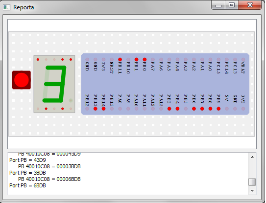
If you want to see the SWD transactions, try setting swd.VERBOSE to True:
SWD interface: FT232H device in Single RS232-HS
Reporta

Rd 0 IDCODE  1BA01477 Ack 1
Wr 0 ABORT   0000001E Ack 1
Wr 4 CTRL    50000000 Ack 1
Rd 4 STATUS  F0000040 Ack 1
DP ident: 1BA01477
Wr 8 SELECT  000000F0 Ack 1
Rd C DRW/BD3 00003BDB Ack 1
Rd C DRW/BD3 14770011 Ack 1
AP ident: 14770011
Wr 8 SELECT  00000000 Ack 1
Wr 0 CSW/BD0 22000002 Ack 1
Wr 4 TAR/BD1 40010C08
Rd C DRW/BD3
Rd C DRW/BD3
Wr 4 TAR/BD1 40010C08 Ack 1
Rd C DRW/BD3 14770011 Ack 1
Rd C DRW/BD3 000043D9 Ack 1
..and so on..
Looking at the last block of 6 transactions, the first 3 are a write-cycle to the SWD TAR (transfer address) register, then a dummy read and the actaul read cycle. These are the requests being sent to the target system; nothing is being read back so the read-data & ack-status values are unknown. The second block of 3 are the readback of these requests, so the actual values are displayed.
An ‘ack’ value of anything apart from 1 is an error; a value of 0 or 7 suggests the target isn’t responding, 2 means it is trying to send a delayed response, and 4 indicates a hard error – this is sticky, so will persist until cleared by writing to the ‘abort’ register.
reporta.py:   main program
rp_pyqt.py:   PyQt interface
rp_arm.py:    ARM processor definitions
rp_swd.py:    SWD interface
rp_ftd2xx.py: FTDI device driver
The lower 3 files are very similar to their counterparts in these posts, basically I’ve copied the files with minor modifications. Each file has a ‘main’ function to demonstrate its functionality; for example, you can see the PyQt interface running without the FTDI hardware, just by executing rp_pyqt.py
The main ‘reporta’ program has no command-line options, currently the I/O port of interest is hard-coded; to add other ports (or CPU memory locations) to the polling list, just use the poll_add_var function.
As with the previous posts, I must state that so far I’ve only tested this technique on the STM32F103 processors; others may require custom powerup sequences, or special incantations to gain access to the CPU memory – but hopefully my Python code will provide a useful starting-point.
Copyright (c) Jeremy P Bentham 2018. Please credit this blog if you are using the information or software in it.
In part 4 we got as far as reading in the CPU identification, which is of no real use; in this part we’ll actually read some of the CPU internals, but first we need to understand how SWD accesses are controlled.
SWD cable showing resistor
DAP: DP and AP
You may think that we just need to feed a 32-bit address into the SWD port, and get a value back, but the reality is much more complicated. The SWD clock & data lines are connected to the CPU Debug Port (SW-DP), which has its own address space. Read/write accesses to the CPU memory aren’t controlled by the DP; you have to go through the Access Port (AP), which also has a separate memory space, and is bank-switched.
DP
We’ve already accessed the Debug Port ID code register, the other read-write registers are:
# Debug Port (SWD-DP) registers
# See ARM DDI 0314H "Coresight Components Technical Reference Manual"
DPORT_IDCODE        = 0x0   # ID Code / abort
DPORT_ABORT         = 0x0
DPORT_CTRL          = 0x4   # Control / status
DPORT_STATUS        = 0x4
DPORT_SELECT        = 0x8   # Select
DPORT_RDBUFF        = 0xc   # Read buffer
These registers control various aspects of the debug interface, for example the ‘abort’ register is used to reset the internal logic after an error, and the ‘control’ register is used to power up the peripherals needed for debugging.
The ‘select’ register has bitfields to control AP and DP bank-switching; it is convenient to define this using CTYPES:
The union allows us to specify the whole 32–bit register when doing SPI read & write cycles, but still access individual bitfields within it.
AP
The AP registers are:
# Access Port (AHB-AP) registers, high nybble is bank number
# See ARM DDI 0337E: Cortex M3 Technical Reference Manual page 11-38
APORT_CSW           = 0x0   # Control status word
APORT_TAR           = 0x4   # Transfer address
APORT_DRW           = 0xc   # Data read/write
APORT_BANK0         = 0x10  # Banked registers
APORT_BANK1         = 0x14
APORT_BANK2         = 0x18
APORT_BANK3         = 0x1c
APORT_DEBUG_ROM_ADDR= 0xf8   # Address of debug ROM
APORT_IDENT         = 0xfc   # AP identification
The Control Status Word register controls various aspects of the CPU memory accesses, for example the data size, and auto-increment for reading blocks of memory:
Because the AP can be accessing main CPU memory, it has two time-dependencies:
the AP may return a ‘wait’ indication in the status field so the transaction has time to go though
the data isn’t returned immediately; first you have to do a dummy read cycle, then a second read cycle that actually returns the data
So to set up a CPU memory read cycle, we need to configure the AP (including its bank-switching) then set a transfer address
# Configure AP memory accesses
def ap_config(d, inc, size):
dp_select.reg.APBANKSEL = 0 # Zero bank
swd.swd_wr(d, swd.SWD_DP, DPORT_SELECT, dp_select.value)
ap_csw.reg.MasterType = 1
ap_csw.reg.HProt1 = 1 # Enable incrementing, set access size
ap_csw.reg.AddrInc = 1 if inc else 0
ap_csw.reg.Size = 0 if size==8 else 1 if size==16 else 2
return swd.swd_wr(d, swd.SWD_AP, APORT_CSW, ap_csw.value)
# Set AP memory address
def ap_addr(d, addr):
swd.swd_wr(d, swd.SWD_AP, APORT_TAR, addr)
swd.swd_idle_bytes(d, 2) # Idle to avoid 'wait' response
# Do an immediate read of a 32-bit CPU memory location
def cpu_mem_read32(d, addr):
ap_addr(d, addr) # Address to read
swd.swd_rd(d, swd.SWD_AP, APORT_DRW) # Dummy read cycle
r = swd.swd_rd(d, swd.SWD_AP, APORT_DRW) # Read data
return r.data.value if r.ack.value==swd.SWD_ACK_OK else None
There are 2 idle (null) bytes after the target memory address is set. These give the AP time to process the address value before it is used; if omitted, the AP gives an ack value of 2 (‘wait’) on the next transaction.
User interface
The console-based user interface is minimal; it just allows you to specify the STM32F103 GPIO port or memory address to be accessed, e.g.
python ftdi_py_part5.py gpiob
DP ident: ack 1, value 1BA01477h
Powerup: ack 1, value F0000040h
AP ident: ack 1, value 14770011h
40010C00: GPIOB CRL=44488433 CRH=33333344 IDR=00007FDA ODR=00007C1A
python ftdi_py_part5.py 0
DP ident: ack 1, value 1BA01477h
Powerup: ack 1, value F0000040h
AP ident: ack 1, value 14770011h
00000000: 20005000
If a gpio port is specified, four of its register values are printed out (CRL, CRH, IDR, ODR); the other diagnostic values can be useful if the access fails. Further help is available by setting the VERBOSE flag at the top of the part 4 file, which enables a printout of all the SWD cycles:
# Command line with invalid address
python ftdi_py_part5.py 800000
Rd 0 IDCODE 1BA01477 Ack 1
DP ident: ack 1, value 1BA01477h
Wr 0 ABORT 0000001E Ack 1
Wr 4 CTRL 50000000 Ack 1
Rd 4 STATUS F0000000 Ack 1
Powerup: ack 1, value F0000000h
Wr 8 SELECT 000000F0 Ack 1
Rd C DRW/BD3 00000000 Ack 1
Rd C DRW/BD3 14770011 Ack 1
AP ident: ack 1, value 14770011h
Wr 8 SELECT 00000000 Ack 1
Wr 0 CSW/BD0 22000012 Ack 1
Wr 4 TAR/BD1 00800000 Ack 1
Rd C DRW/BD3 14770011 Ack 1
Rd C DRW/BD3 00000000 Ack 4
00800000: ?
Source code
Here is the final batch of source-code. I’ve only tested the it with STM32F1 CPUs, so if you are trying to communicate with something else, there is a strong possibility you’ll need to make some changes. Points to bear in mind:
Check the the CPU supports SWD, and the connections it uses.
Check for any special power-up requirements, e.g. sending the reset sequence multiple times, or setting registers to enable debugging mode
Check that the SWD clock and signal lines are toggling OK.
Watch out for acknowledgement values 2 and 4, indicating a problem.
Once an error occurs, it will persist over successive cycles until reset by writing to the ABORT register.
Good luck!
# Python FTDI SWD CPU memory read from iosoft.blog
# Compatible with Python 2.7 or 3.x
#
# v0.01 JPB 8/12/18
import sys, ftdi_py_part3 as ft, ftdi_py_part4 as swd
from ctypes import Structure, Union, c_uint
# STM32F1 address values for testing
# Address of GPIO Ports A - E on STM32F1
ports = {"GPIOA":0x40010800, "GPIOB":0x40010C00, "GPIOC":0x40011000,
"GPIOD":0x40011400, "GPIOE":0x40011800}
# GPIO registers at offsets 0, 4, 8, 12
gpio_regs = ("CRL", "CRH", "IDR", "ODR")
# Debug Port (SWD-DP) registers
# See ARM DDI 0314H "Coresight Components Technical Reference Manual"
DPORT_IDCODE = 0x0 # ID Code / abort
DPORT_ABORT = 0x0
DPORT_CTRL = 0x4 # Control / status
DPORT_STATUS = 0x4
DPORT_SELECT = 0x8 # Select
DPORT_RDBUFF = 0xc # Read buffer
# Access Port (AHB-AP) registers, high nybble is bank number
# See ARM DDI 0337E: Cortex M3 Technical Reference Manual page 11-38
APORT_CSW = 0x0 # Control status word
APORT_TAR = 0x4 # Transfer address
APORT_DRW = 0xc # Data read/write
APORT_BANK0 = 0x10 # Banked registers
APORT_BANK1 = 0x14
APORT_BANK2 = 0x18
APORT_BANK3 = 0x1c
APORT_DEBUG_ROM_ADDR= 0xf8 # Address of debug ROM
APORT_IDENT = 0xfc # AP identification
# DP Select Register
class DP_SELECT_REG(Structure):
_fields_ = [("DPBANKSEL", c_uint, 4),
("APBANKSEL", c_uint, 4),
("Reserved", c_uint, 16),
("APSEL", c_uint, 8)]
class DP_SELECT(Union):
_fields_ = [("reg", DP_SELECT_REG),
("value", c_uint)]
dp_select = DP_SELECT()
# AHB-AP Control Status Word Register
class AP_CSW_REG(Structure):
    _fields_ = [("Size", c_uint, 3),
                ("Res1", c_uint, 1),
                ("AddrInc", c_uint, 2),
                ("DbgStatus", c_uint, 1),
                ("TransInProg", c_uint, 1),
                ("MODE", c_uint, 4),
                ("Res2", c_uint, 13),
                ("HProt1", c_uint, 1),
                ("Res3", c_uint, 3),
                ("MasterType", c_uint, 1),
                ("Res4", c_uint, 2)]
class AP_CSW(Union):
    _fields_ = [("reg", AP_CSW_REG),
                ("value", c_uint)]
ap_csw = AP_CSW()
# Select AP bank, do read cycle
def ap_banked_read(d, addr):
dp_select.reg.APBANKSEL = addr >> 4;
swd.swd_wr(d, swd.SWD_DP, DPORT_SELECT, dp_select.value)
swd.swd_rd(d, swd.SWD_AP, addr&0xf)
return swd.swd_rd(d, swd.SWD_AP, addr&0xf)
# Configure AP memory accesses
def ap_config(d, inc, size):
    dp_select.reg.APBANKSEL = 0     # Zero bank
    swd.swd_wr(d, swd.SWD_DP, DPORT_SELECT, dp_select.value)
    ap_csw.reg.MasterType = 1
    ap_csw.reg.HProt1 = 1           # Enable incrementing, set access size
    ap_csw.reg.AddrInc = 1 if inc else 0
    ap_csw.reg.Size = 0 if size==8 else 1 if size==16 else 2
    return swd.swd_wr(d, swd.SWD_AP, APORT_CSW, ap_csw.value)

# Set AP memory address
def ap_addr(d, addr):
    swd.swd_wr(d, swd.SWD_AP, APORT_TAR, addr)
    swd.swd_idle_bytes(d, 2)            # Idle to avoid 'wait' response

# Do an immediate read of a 32-bit CPU memory location
def cpu_mem_read32(d, addr):
    ap_addr(d, addr)                              # Address to read
    swd.swd_rd(d, swd.SWD_AP, APORT_DRW)          # Dummy read cycle
    r = swd.swd_rd(d, swd.SWD_AP, APORT_DRW)      # Read data
    return r.data.value if r.ack.value==swd.SWD_ACK_OK else None
if __name__ == "__main__":
mem = sys.argv[1].upper() if len(sys.argv) > 1 else None
dev = ft.ft_open()
if not dev:
print("Can't open FTDI device")
sys.exit(1)
ft.set_bitmode(dev, 0, 2) # Enable SPI
ft.set_spi_clock(dev, 1000000) # Set SPI clock
ft.ft_write(dev, (0x80, 0, ft.OPS)) # Set outputs
swd.swd_reset(dev) # Send SWD reset sequence
resp = swd.swd_rd(dev, swd.SWD_DP, DPORT_IDCODE) # Request & response
if resp is None:
print("No response")
else:
print("DP ident: ack %u, value %08Xh" % (resp.ack.value, resp.data.value))
swd.swd_wr(dev, swd.SWD_DP, DPORT_ABORT, 0x1e) # Clear errors
swd.swd_wr(dev, swd.SWD_DP, DPORT_CTRL, 0x5<<28) # Powerup request
resp = swd.swd_rd(dev, swd.SWD_DP, DPORT_STATUS) # Get status
print("Powerup: ack %u, value %08Xh" % (resp.ack.value, resp.data.value))
resp = ap_banked_read(dev, APORT_IDENT) # Get AP ident
print("AP ident: ack %u, value %08Xh" % (resp.ack.value, resp.data.value))
ap_config(dev, 1, 32); # Configure AP RAM accesses
s = ""
if mem in ports:
addr = ports[mem]
s = "%08X: %s" % (addr, mem)
for reg in gpio_regs:
val = cpu_mem_read32(dev, addr)
s += " %s=%08X" % (reg, val)
addr += 4
else:
try:
addr = int(mem, 16)
except:
addr = None
if addr is not None:
s = "%08X:" % addr
val = cpu_mem_read32(dev, addr)
s += " %08X" % val if val is not None else " ?"
print(s)
dev.close()
# EOF
Next steps
Whilst this code is an interesting framework for experimentation, it lacks some of the features and error-handling of a ‘real’ application, for example it’d be nice to draw an animated picture of the CPU, showing the SWD poll results graphically. That is the subject of another post.
Copyright (c) Jeremy P Bentham 2018. Please credit this blog if you are using the information or software in it.
If you want to access the internals of a programmable device, there used to be only one way: a JTAG interface. This uses 4 signals: TDI, TDO, TCK and TMS, and is quite complex; it can handle multiple daisy-chained devices, of various types. When you add in a variety of USB-JTAG adaptors and APIs to serve data to higher-level GUIs, you have a very complex piece of software; for an illustration of this, take a look at OpenOCD
More recently, ARM introduced a simpler 2-wire protocol, called SWD. It has just 2 connections, clock and bi-directional data, but has most of the capabilities of the older JTAG systems. Software such as OpenOCD has been extended to incorporate the SWD protocol, but is still very complex; I felt there was a need for a simple-as-possible implementation, in a high-level language, that could easily be combined with custom GUI to display the CPU internals in whatever fashion suits your application; maybe an animated diagram of the CPU, display of serial data streams, or graphs of analogue values.
So the Python SWD project was born, and I needed to select a USB device for the interface. The more modern FTDI parts have the MPSSE protocol engine, which (as we’ll see later) is ideally suited for the SWD protocol, and there are a wide variety of FTDI cables and modules at reasonable cost.
In the previous blog posts I’ve documented some preliminary steps to understand the FTDI hardware, and how it can be driven from Python; now we have a major test, implementing the SWD protocol.
Hardware
FTDI adaptors
We’ll only be using 3 pins (clock, data out, data in) on the adaptor, so it isn’t difficult to wire up and FTDI cable or module, the only requirements are that the device supports the MPSSE protocol, and has a 3.3V output. If the module has a 5 volt pin, you do need to be careful not to short-circuit or mis-connect it, as it can source quite high currents (over an amp) and do significant damage. If you peer closely at the above diagram, you’ll see top-right an Adafruit FT232H module with connector pins fitted but missing pin 1; this is so I can’t accidentally destroy my test CPU by accidentally connecting the SWD to 5 volts.
In the introduction I mentioned that the SWD protocol has a bi-directional data line, but unfortunately the FTDI adaptors don’t provide a bi-directional mode – we need to combine the data input & output lines to provide this. This is done by putting a resistor in series with the FTDI output, so that the target system can pull that line high or low when required.
SWD cable circuit diagram
SWD cable with heatshrink pulled back to show DI-DO resistor
A similar scheme is mentioned in the OpenOCD documentation, but they suggest a value of 470 ohms. I’ve gone with 1K because at its lowest drive setting, FTDI chips such as the FT232H only source 4 mA, and I’m never keen on overloading outputs, no matter how harmless this is supposed to be – but feel free to follow the majority opinion, and go with 470 ohms.
Some people suggest that is is necessary for the FTDI adaptor and target CPU to share a common supply. Professional JTAG adaptors do this – they take a supply from the target system, and use level-shifters to ensure the signals are of the right amplitude – but it should’t be necessary providing your supplies are of reasonable quality. However, you must resist the temptation to make the cables very long; we’re dealing with fast edge-sensitive signals, so I’d keep the cable length below 6 inches (150 mm).
A convenient way of incorporating the resistor in a cable is by soldering & covering with heat-shrink tubing; at a pinch you could use a screw-terminal block, but try to keep the assembly reasonably compact to avoid EMC problems.
SWD Protocol
There are 3 main difficulties with this protocol:
Bit-oriented rather than byte-oriented
Bi-directional data line
Intolerant of errors
The first of these is quite a culture-shock; when dealing with bit values, they are usually aggregated up to the nearest byte or word. This isn’t good enough for SWD; if you are supposed to be sending 2 bits, it must be 2 bits, not padded out to the nearest byte.
The second issue makes debugging the software quite challenging; if there is a bug that causes both sides to transmit at the same time, it is difficult to work out which side is at fault.
The third issue is actually a design feature; in the event of an error, the CPU interface is designed to stop transmitting, to avoid further data collisions – but when writing your own code, you often find the target CPU stops talking; it refuses to communicate, and you don’t know why.
To give an example, here is the standard SWD read transaction on which all data transfers are based, taken from the original ARM document “Serial Wire Debug and the CoreSight Debug and Trace Architecture”. All transactions are initiated and controlled by the SWD adaptor, the target CPU just ‘fills in the blanks’ in the messages it is given.
We start with the data line being idle, which (very confusingly) can be either high or low. The clock line can be either be running continuously, or can stop between transactions; a bit like Ethernet, in that the recipient looks for a specific marker in the data, and ignores everything until that is received. In this context, the marker is at least 2 low (zero) bits, followed by a high ‘start’ bit, then there are 7 bits of header data. If you want to know the meaning of these bits, ARM have copious online documentation, such as the “CoreSight Components Technical Reference Manual”.
After the initial transmission to the CPU, the adaptor inserts a dummy ‘turnaround’ bit where it stops driving the data line, letting the target CPU take over. The adaptor continues toggling the clock line while the CPU sends 3 acknowledgement bits; if these show a positive response (100, l.s.bit first, so a value of 1) then 32 bits of data will follow, and a parity bit. This concludes the transaction, but another turnaround bit is needed so the SWD adaptor can start driving the bus again.
Alternatively, the acknowledgement bits may show an error (001, which is a value of 4), in which case the CPU will stop communicating, or a ‘wait’ indication (010, a value of 2), which means the data isn’t yet available – try again later.
After this transaction, another may follow immediately, or a minimum of 2 zero bits may be inserted to idle the data line – a clean transition between transactions is essential, with no spurious additional bits.
Python implementation
After several false starts, I ended up creating my own class to store bit values; there are various bit-handling libraries around, but my requirements are so simple that these are massive overkill.
# Class for a multi-bit value
class Bitval(object):
    def __init__(self, value, nbits, name="", rd=False):
        self.value = value
        self.nbits = nbits
        self.name = name
        self.rd = rd
That’s all – it is just a vehicle for storing one or more bits; the ‘name’ isn’t strictly necessary, but is useful in identifying one bit-value amongst many others.
The ‘rd’ flag indicates whether the value should be write-only, or whether we need the value to be read back from the target system. For example, in the SWD read cycle above, we need to know the ‘ack’ and ‘data’ values, but aren’t really interested in reading back the other bits we’re sending – and the FTDI device provides a convenient way of controlling whether input data is read back or not (command bit 5: ‘TDO/DI data input’).
Creating the SWD request is just a question of stacking the bit-values in a list, e.g.
Our USB driver software just churns out the bit-values in sequence, then gets any responses that are required; it doesn’t need to understand what each bit-value means. All that is needed is a bit of support code, to allow iteration through the list, and give access to the important element values:
# Create an SWD read request for a given AP or DP address
class swd_rd_request(object):
    def __init__(self, ap, addr):
        addr >>= 2
        hpar = ap ^ 1 ^ (addr & 1) ^ (addr>>1 & 1)
        self.ack = Bitval(0, 3, "Ack", 1)
        self.data = Bitval(0, 32, "Data", 1)
        self.dparity = Bitval(0, 1, "DParity", 1)
        self.bitvals = (
            Bitval(1, 1, "Start"),      Bitval(ap, 1, "AP"),
            Bitval(1, 1, "Read"),       Bitval(addr, 2, "Addr"),
            Bitval(hpar, 1, "HParity"), Bitval(0, 1, "Stop"),
            Bitval(1, 1, "Park"),       Bitval(0, 1, "Turn"),
            self.ack,                   self.data,
            self.dparity,               Bitval(0, 1, "Turn"))

    # Allow the bitval list to be iterated
    def __getitem__(self, idx):
        bv = self.bitvals[idx]
        return bv
Having set up a class for our data transaction, it is easy to transmit the data, and evaluate the response:
req = swd_rd_request(ap, addr)  # Create request
for bv in req:                  # For each bit-value..
    spi_write_bitval(h, bv)     # ..send bit(s) out
for bv in req:                  # For each bit-value..
    if bv.rd:                   # .. with 'rd' flag set..
        spi_read_bitval(h, bv)  # .. read bit(s) in
Since the request is a class instance, we can access the returned bits in an intuitive way, e.g. simplistically:
if req.ack.value == 1:     # If request was acknowledged OK..
    print(req.data.value)  # ..print returned data value
SWD reset
Now that we have an easy way to send an SWD request, can we read something out from the CPU? Nearly, there is just the reset process to go through.
To unlock the CPU SWD interface and start communicating, we need to send a lengthy bit sequence, namely at least 50 ‘1’ bits, then 0111 1001 1110 0111 (9E E7 hex, l.s.bit first), then at least another 50 ‘1’ bits, then at least 2 ‘0’ bits. this serves 2 purposes:
It provides a unique bit-pattern, that can’t be confused with a normal request
It gives time for the CPU SWD interface to be powered up
The second point is important; ARM CPUs are designed with power-saving in mind, and parts of the CPU may be powered down when not in use, so need some time to wake up. This especially applies if the CPU is in a deep sleep mode; it may require the startup sequence to be sent several times before the CPU is sufficiently awake to respond to requests. Despite the ‘reset’ name, this sequence does not reset the error-handling of the SWD interface; that must be done using a separate write-cycle.
Reading the CPU ID
After sending the startup sequence, the first request should be a read of the CPU ID; not just because it is a simple read-only value, but also because the CPU specification may require that it be read before anything else.
We need to set the ‘ap’ and ‘addr’ values in the code above; I’ll describe these settings in detail in the next post, but for now, it is sufficient to say that the ID register is at DP address 0, so ap=0, addr = 0.
So we just need to send the startup bit pattern, then a request with these values, and read back the result. If we’re unlucky, it’ll be all-0s because the target CPU isn’t communicating, or all-1s because the data line is floating; ideally it is something between those, that is consistent every time it is read; on an STMicro Cortex M3 CPU (STM32F103) it is 1BA01477, see your CPU’s data sheet for the corresponding value.
See below for the full Python source code to read the ID register; I can’t claim this code is particularly useful on its own, but in the next post we’ll start to explore some more useful data requests.
Regrettably the code doesn’t work on Linux with libftdi. In all my tests the SPI write cycles work fine, but the read cycles always return null data. To be investigated.
# Python FTDI SWD example from iosoft.blog
# Compatible with Python 2.7 or 3.x
#
# v0.01 JPB 8/12/18

import time, ftdi_py_part3 as ft

VERBOSE  = False    # Flag to display SWD read/write cycles
ERRVAL = 0xEEEEEEEE # Dummy value returned if read cycle fails

SWD_DP          = 0     # AP/DP flag bits
SWD_AP          = 1
DPORT_IDCODE    = 0x0   # ID Code address

SWD_ACK_OK      = 1     # SWD Ack values
SWD_ACK_WAIT    = 2
SWD_ACK_ERROR   = 4

FTDI_MODE_BITBANG   = 1     # MPSSE modes
FTDI_MODE_MPSSE     = 2

FTDI_SPI_WR_CLK_NEG = 0x01  # SPI command bit values
FTDI_SPI_BIT_MODE   = 0x02
FTDI_SPI_RD_CLK_NEG = 0x04
FTDI_SPI_LSB_FIRST  = 0x08
FTDI_SPI_WR_TDI     = 0x10
FTDI_SPI_RD_TDO     = 0x20
FTDI_SPI_WR_TMS     = 0x40

# Commands to read, write, and read+write SPI data
SPI_WR_BYTES    = FTDI_SPI_WR_CLK_NEG|FTDI_SPI_LSB_FIRST|FTDI_SPI_WR_TDI
SPI_RD_BYTES    = FTDI_SPI_LSB_FIRST|FTDI_SPI_RD_TDO
SPI_RD_WR_BYTES = SPI_RD_BYTES|SPI_WR_BYTES
SPI_RD_BITS     = SPI_RD_BYTES|FTDI_SPI_BIT_MODE
SPI_WR_BITS     = SPI_WR_BYTES|FTDI_SPI_BIT_MODE
SPI_RD_WR_BITS  = SPI_RD_BITS|SPI_WR_BITS

# Class for a bit value (1 - 32 bits)
class Bitval(object):
    def __init__(self, value, nbits, name="", rd=False):
        self.value = value
        self.nbits = nbits
        self.name = name
        self.rd = rd

# Send SWD reset; at least 50 high bits around 0111 1001 1110 0111
# (9E E7 lsb-first), then at least 2 null bits before start bit
def swd_reset(d):
    rst = (0xFF,0xFF,0xFF,0xFF,0xFF,0xFF,0xFF, 0x9E,0xE7,
           0xFF,0xFF,0xFF,0xFF,0xFF,0xFF,0xFF)
    spi_write_bytes(d, SPI_WR_BYTES, rst)
    spi_write_bits(d, SPI_WR_BITS, 0, 4)

# Send a number of idle (zero) bytes
def swd_idle_bytes(d, n):
    data = n * [0]
    spi_write_bytes(d, SPI_WR_BYTES, data)

# Create an SWD read request for a given AP or DP address
class swd_rd_request(object):
    def __init__(self, ap, addr):
        addr >>= 2
        hpar = ap ^ 1 ^ (addr & 1) ^ (addr>>1 & 1)
        self.ack = Bitval(0, 3, "Ack", 1)
        self.data = Bitval(0, 32, "Data", 1)
        self.dparity = Bitval(0, 1, "DParity", 1)
        self.bitvals = (
            Bitval(1,    1, "Start"),  Bitval(ap,   1, "AP"),
            Bitval(1, 1, "Read"),      Bitval(addr, 2, "Addr"),
            Bitval(hpar, 1, "HParity"),Bitval(0, 1, "Stop"),
            Bitval(1,    1, "Park"),   Bitval(0,    1, "Turn"),
            self.ack,                  self.data,
            self.dparity,              Bitval(0, 1, "Turn"))

    # Allow the bitval list to be iterated
    def __getitem__(self, idx):
        bv = self.bitvals[idx]
        return bv

# Create an SWD write request for a given AP or DP address
class swd_wr_request(object):
    def __init__(self, ap, addr, value):
        addr >>= 2
        hpar = ap ^ (addr & 1) ^ (addr>>1 & 1)
        self.ack = Bitval(0, 3, "Ack", 1)
        self.data = Bitval(value, 32, "Data")
        self.dparity = Bitval(parity32(value), 1, "DParity")
        self.bitvals = (
            Bitval(1,    1, "Start"),  Bitval(ap,   1, "AP"),
            Bitval(0, 1, "Read"),      Bitval(addr, 2, "Addr"),
            Bitval(hpar, 1, "HParity"),Bitval(0, 1, "Stop"),
            Bitval(1,    1, "Park"),   Bitval(0,    1, "Turn"),
            self.ack,                  Bitval(0,    1, "Turn"),
            self.data,                 self.dparity)

    # Allow the bitval list to be iterated
    def __getitem__(self, idx):
        bv = self.bitvals[idx]
        return bv

# Send an SWD read request and/or get the response
def swd_rd(d, ap, addr, tx=True, rx=True):
    req = swd_rd_request(ap, addr)
    ok = False
    if tx:
        spi_write_bitvals(d, req)
        ok = True
    if rx:
        ok = spi_read_bitvals(d, req)
    if VERBOSE:
        if rx:
            print("  Rd %X %-7s %08lX Ack %u" % (addr,
                  apreg_str(addr) if ap else dpreg_str(addr, 1),
                  req.data.value, req.ack.value))
        else:
            print("  Rd %X %-7s" % (addr,
                  apreg_str(addr) if ap else dpreg_str(addr, 1)))
    return req if ok else None

# Send an SWD write request and/or get the response
def swd_wr(d, ap, addr, value, tx=True, rx=True):
    req = swd_wr_request(ap, addr, value)
    ok = False
    if tx:
        spi_write_bitvals(d, req)
        ok = True
    if rx:
        ok = spi_read_bitvals(d, req)
    if VERBOSE:
        if rx:
            print("  Wr %X %-7s %08lX Ack %u" % (addr,
                  apreg_str(addr) if ap else dpreg_str(addr, 0),
                  req.data.value, req.ack.value))
        else:
            print("  Wr %X %-7s %08lX" % (addr,
                  apreg_str(addr) if ap else dpreg_str(addr, 0),
                  req.data.value))
    return req if ok else None

# Return DP register string
def dpreg_str(reg, rd):
    if rd:
        s = ("IDCODE" if reg==0 else "STATUS" if reg==4 else
             "RESEND" if reg==8 else "RDBUFF")
    else:
        s = ("ABORT " if reg==0 else "CTRL" if reg==4 else
             "SELECT" if reg==8 else "RDBUFF")
    return s

# Return AP register string; see Cortex-M3 'AHB-AP programmers model'
def apreg_str(reg):
    return ("CSW/BD0" if reg==0 else "TAR/BD1" if reg==4 else
            "BD2/RAR" if reg==8 else "DRW/BD3")

# Write bitval requests
def spi_write_bitvals(d, bitvals):
    for bv in bitvals:
        spi_write_bitval(d, bv)

# Read bitval responses
def spi_read_bitvals(d, bitvals):
    ok = True
    for bv in bitvals:
        ok = spi_read_bitval(d, bv)
        if not ok:
            break
    return ok

# Write a bit value to SPI interface
# If read-flag is set, use read+write, otherwise just write
def spi_write_bitval(d, bv):
    value, nbits = bv.value, bv.nbits
    cmd = SPI_RD_WR_BITS if bv.rd else SPI_WR_BITS
    while nbits > 0:
        n = min(nbits, 8)
        spi_write_bits(d, cmd, value&0xff, n)
        value >>= n
        nbits -= n

# Read a bit value (max 32 bits) from SPI, if read-flag is set
def spi_read_bitval(d, bv):
    ok = True
    if bv.rd:
        bv.value = shift = 0
        nbits = bv.nbits
        while ok and nbits >= 8:    # Get whole bytes
            data = spi_read_bytes(d, 1)
            if len(data) > 0:
                byt = data[0] >> max(8-nbits, 0)
                bv.value |= byt  0:
                bv.value = data[0]
            else:
                bv.value = ERRVAL
                ok = False
    return ok

# Write SPI command and data bytes to the device
def spi_write_bytes(d, cmd, data):
    n = len(data) - 1
    ft.ft_write(d, [cmd, n&0xff, n>>8] + list(data))

# Read data bytes back from SPI
def spi_read_bytes(d, nbytes):
    return ft.ft_read(d, nbytes)

# Write SPI command and up to 8 bits to the device
def spi_write_bits(d, cmd, byt, nbits):
    ft.ft_write(d, (cmd, nbits-1, byt))

# Read data bits back from SPI
# Bits are left-justified in the byte, so must be shifted down
def spi_read_bits(d, nbits):
    data = ft.ft_read(d, 1)
    return [data[0] >> (8-nbits)] if len(data)>0 else []

# Calculate parity of 32-bit integer
def parity32(i):
    i = i - ((i >> 1) & 0x55555555)
    i = (i & 0x33333333) + ((i >> 2) & 0x33333333)
    i = (((i + (i >> 4)) & 0x0F0F0F0F) * 0x01010101) >> 24
    return i & 1

if __name__ == "__main__":
    dev = ft.ft_open()
    if not dev:
        print("Can't open FTDI device")
    else:
        ft.set_bitmode(dev, 0, 2)           # Enable SPI
        ft.set_spi_clock(dev, 1000000)      # Set SPI clock
        ft.ft_write(dev, (0x80, 0, ft.OPS)) # Set outputs
        swd_reset(dev)                      # Send SWD reset sequence
        r = swd_rd(dev, SWD_DP, DPORT_IDCODE) # Request & response
        if r is None:
            print("No response")
        else:
            print("SWD ack %u, ID %08Xh" % (r.ack.value, r.data.value))
        dev.close()
# EOF
In the next post we’ll be doing something a bit more useful – accessing the CPU address space.
Copyright (c) Jeremy P Bentham 2018. Please credit this blog if you use the information or software in it.